Chips
I love Integrated Circuits (chips) so this is a page about them.
This Months HOT MCU
STM32F7x7
Arm® 32-bit Cortex®-M7 CPU
Up to 2 Mbytes of Flash
SRAM: 512 Kbytes,
16 Kbytes I/D cache, allowing 0-wait state execution from embedded Flash and external memories, up to 216 MHz
462 DMIPS/2.14 DMIPS/MHz (Dhrystone 2.1)
DSP instructions
Download STM32F777-technical-manual
This is my HOT MCU choice for August, the STM32F7x7 MCU.
Features
· Memories
Up to 2 Mbytes of Flash memory organized
into two banks allowing read-while-write
SRAM: 512 Kbytes (including 128 Kbytes
of data TCM RAM for critical real-time data)
+ 16 Kbytes of instruction TCM RAM (for
critical real-time routines) + 4 Kbytes of
backup SRAM
Flexible external memory controller with up
to 32-bit data bus: SRAM, PSRAM,
SDRAM/LPSDR SDRAM, NOR/NAND
memories
· Dual mode Quad-SPI
· Graphics
Chrom-ART AcceleratorTM (DMA2D),
graphical hardware accelerator enabling
enhanced graphical user interface
Hardware JPEG codec
LCD-TFT controller supporting up to XGA
resolution
MIPI® DSI host controller supporting up to
720p 30 Hz resolution
· Clock, reset and supply management
1.7 V to 3.6 V application supply and I/Os
POR, PDR, PVD and BOR
Dedicated USB power
4-to-26 MHz crystal oscillator
Internal 16 MHz factory-trimmed RC (1%
accuracy)
32 kHz oscillator for RTC with calibration
Internal 32 kHz RC with calibration
· Low-power
Sleep, Stop and Standby modes
VBAT supply for RTC, 32×32 bit backup
registers + 4 Kbytes backup SRAM
· 3×12-bit, 2.4 MSPS ADC: up to 24 channels
· Digital filters for sigma delta modulator
(DFSDM), 8 channels / 4 filters
· 2×12-bit D/A converters
· General-purpose DMA: 16-stream DMA
controller with FIFOs and burst support
· Up to 18 timers: up to thirteen 16-bit (1x low-
power 16-bit timer available in Stop mode) and
two 32-bit timers, each with up to 4
IC/OC/PWM or pulse counter and quadrature
(incremental) encoder input. All 15 timers
running up to 216 MHz. 2x watchdogs, SysTick
timer
· Debug mode
SWD & JTAG interfaces
Cortex®-M7 Trace MacrocellTM
· Up to 168 I/O ports with interrupt capability
Up to 164 fast I/Os up to 108 MHz
Up to 166 5 V-tolerant I/Os
· Up to 28 communication interfaces
Up to 4 I2C interfaces (SMBus/PMBus)
Up to 4 USARTs/4 UARTs (12.5 Mbit/s,
ISO7816 interface, LIN, IrDA, modem
control)
Up to 6 SPIs (up to 54 Mbit/s), 3 with
muxed simplex I2S for audio
2 x SAIs (serial audio interface)
3 × CANs (2.0B Active) and 2x SDMMCs
SPDIFRX interface
HDMI-CEC
MDIO slave interface
· Advanced connectivity
USB 2.0 full-speed device/host/OTG
controller with on-chip PHY
USB 2.0 high-speed/full-speed
device/host/OTG controller with dedicated
DMA, on-chip full-speed PHY and ULPI
10/100 Ethernet MAC with dedicated DMA:
supports IEEE 1588v2 hardware, MII/RMII
· 8- to 14-bit camera interface up to 54 Mbyte/s
· Cryptographic acceleration: hardware
acceleration for AES 128, 192, 256, triple DES,
HASH (MD5, SHA-1, SHA-2), and HMAC
· True random number generator
· CRC calculation unit
· RTC: subsecond accuracy, hardware calendar
· 96-bit unique ID
A Most Beautiful Chip, the STM32L162RD
These are some pics I took with my cheap USB microscope, so they are not that special, but hopefully you’ll get the idea.
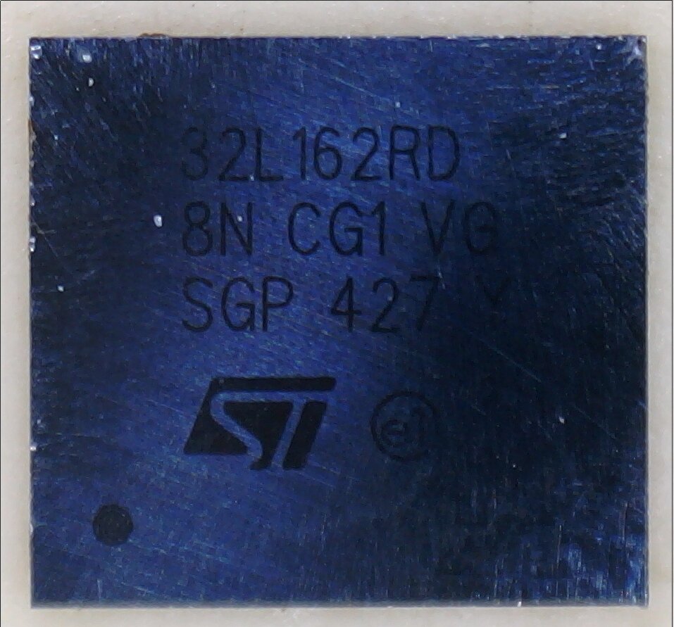
STM32L162RD
This chip has been sitting on my bench for a few months, so I cleaned it as best I could with Metholated Spirits before taking the pics below.
The actual chip came from arrow.com where I purchased 10 units for $0.90 AUD each as they were ‘overstocked’.
The package is a WLCSP64 and is approximately 4.5 mm x 4.5 mm on each side and 0.38 mm thick with 64 solder blobs for pins (BGA).
The entire chip is silicon and the size of the actual DIE, there is no plastic or any other case material, and no copper pins.
This to my mind represents the state of the art in miniaturization, where the connections are via solder blobs onto metallized tracks which connect to the pads on the die periphery.
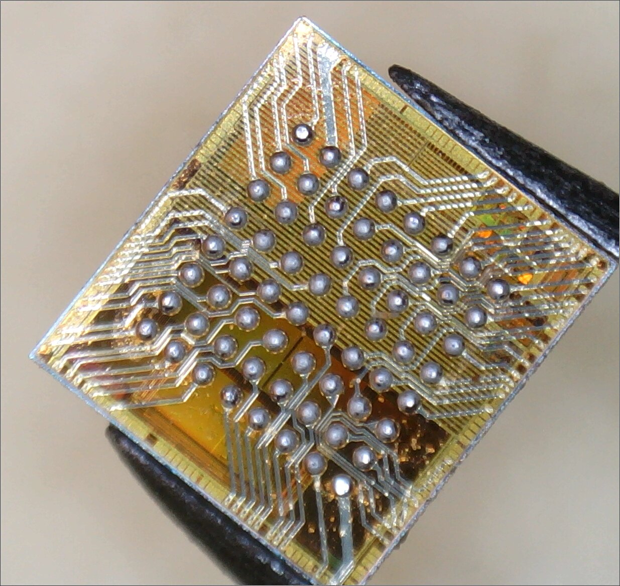
STM32L162RD Bottom
When I looked at this chip under my 40x microscope it took my breath away because I could see under the silver and gold metallization into the chip itself. That’s right, the parallel lines which look a dull gold in my picture, looked shiny and like they are made of solid GOLD in the microscope
I’ve never seen anything as breathtaking as this before and I’m used to looking at chips with microscopes and lighting that make the “wire bonding” wires look the size of lamp posts.
4.5 x 4.5mm chip size, solder balls: 0.4mm apart
STM32L162RD Top
In this picture the laser/etch printing on the top of the chip can be seen. When it was newly taken out of the sealed shipping packaging, the top was like a mirror, flawless. Even after cleaning it’s still nothing like the unblemished new state.
4.5 x 4.5mm chip size
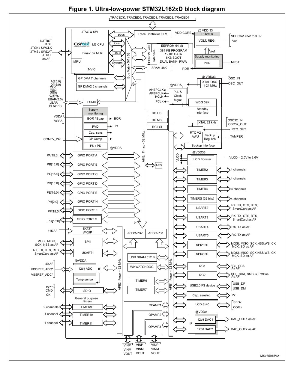
Block Diagram
Capability
This chip is just JAM PACKED with peripherals, it is mind boggling!
Ultra-low-power 32-bit MCU Arm® Cortex®-M3
384KB Flash
48KB SRAM
12KB EEPROM
LCD, USB, ADC, memory I/F, AES
Low Power, 305 nA Standby mode
Features LQFP144 (20 × 20 mm) UFBGA132 WLCSP64
LQFP100 (14 × 14 mm) (7 × 7 mm) (0.4 mm pitch)
· Ultra-low-power platform LQFP64 (10 × 10 mm)
1.65 V to 3.6 V power supply
-40°C to 105°C temperature range · Memories
305 nA Standby mode (3 wakeup pins) 384 Kbytes of Flash memory with ECC
1.15 µA standby mode + RTC (with 2 banks of 192 Kbytes enabling Rww
0.475 µA Stop mode (16 wakeup lines) capability)
1.35 µA Stop mode + RTC 48 Kbytes of RAM
11 µA Low-power run mode 12 Kbytes of true EEPROM with ECC
230 µA/MHz Run mode 128-byte backup register
10 nA ultra-low I/O leakage Memory interface controller supporting
8 µs wakeup time SRAM, PSRAM and NOR Flash
· AES-128 bit encryption hardware accelerator · LCD driver for up to 8x40 segments
· Core: Arm® Cortex®-M3 32-bit CPU Support contrast adjustment
Support blinking mode
From 32 kHz up to 32 MHz max Step-up converter on board
1.25 DMIPS/MHz (Dhrystone 2.1)
Memory protection unit · Rich analog peripherals (down to 1.8V)
3x operational amplifiers
· Reset and supply management 12-bit ADC 1 Msps up to 40 channels
Low-power, ultrasafe BOR (brownout reset) 12-bit DAC 2 ch with output buffers
with 5 selectable thresholds 2x ultra-low-power comparators
Ultra-low-power POR/PDR (window mode and wakeup capability)
Programmable voltage detector (PVD)
· DMA controller 12x channels
· Clock sources
1 to 24 MHz crystal oscillator · 12x peripheral communication interfaces
32 kHz oscillator for RTC with calibration 1x USB 2.0 (internal 48 MHz PLL)
High speed internal 16 MHz factory- 5x USARTs
trimmed RC (+/- 1%) Up to 8x SPIs (2x I2S, 3x 16 Mbit/s)
Internal low power 37 kHz RC 2x I2Cs (SMBus/PMBus)
Internal multispeed low power 65 kHz to 1x SDIO interface
4.2 MHz
PLL for CPU clock and USB (48 MHz) · 11x timers: 1x 32-bit, 6x 16-bit with up to 4
IC/OC/PWM channels, 2x 16-bit basic timers,
· Pre-programmed bootloader 2x watchdog timers (independent and window)
USB and USART supported
· Up to 34 capacitive sensing channels
· Development support
Serial wire debug supported · CRC calculation unit, 96-bit unique ID
JTAG and trace supported
· Up to 116 fast I/Os (102 I/Os 5V tolerant), all
mappable on 16 external interrupt vectors
The Perfect Chip Right?
So is it the perfect chip for embedded usage ?
Probably not, but it’s sure pretty, and perhaps represents the state of the art because I don’t think anything else could be packed into this tiny space.
This type of package is quite fragile, open to light so needs to be sealed underneath after reflow soldering. The solder balls are VERY close to the silver tracks (which may be non conductive on the surface as they cross over each other at a few places on the chip), so I imagine BEST BGA practices would be needed to use it.
I could easily scrape the metallization off the base with a knife using virtually no force tho this is not a fair criticism because I’m a 100 ton giant to this tiny silicon chip.
Runs Mecrisp-Stellaris?
Of course it does, or I wouldn’t have purchased it and made this page.