RCC_PLLCFGR
A funny thing happened to me on my way to the STM32F407 RCC_PLLCFGR
Around the 25th of March this year (2021) I completed rewriting the STM32F407 clock code previously designed by Matthias and others and lately re-writen by Jan Bramkamp to allow more Flash wait states.
I like to rewrite Forth code which uses ‘magic numbers’ to code using the words from my latest svd2forth to better understand the code.
Everything was going fine until I got to this code which does what exactly and why are various bitfields summed together ?
Why are they then saved to RCC_PLLCFGR in the word “pll-168MHz” ?
The pll-168MHz code block
7 24 lshift    \ PLLQ = 7
22 bit +       \ PLLSRC = HSE, PLLP = 0
336 6 lshift + \ PLLN = 336
8 +            \ PLLM = 8
constant pll-8>168

: pll-168MHz ( -- ) pll-8>168 RCC_PLLCFGR ! ;
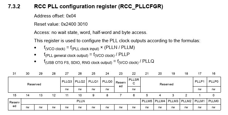
It’s all valid Forth code writen by experts but the layout seemed a bit odd to me. Searching the Technical Ref and bitfields.fs I found these …. WTF ? Look at PLLN in the Technical Ref image, it clearly shows nine bits in the one bitfield, however the SVD lists each bit in its own bitfield!
The Technical Manual doesn’t agree with the SVD ? this can’t be good ?
Technical Ref
bitfields.fs
\ RCC_PLLCFGR (read-write) Reset:0x24003010
: RCC_PLLCFGR_PLLQ3 ( -- x addr ) 27 bit RCC_PLLCFGR ; \ RCC_PLLCFGR_PLLQ3, Main PLL PLL division factor for USB  OTG FS, SDIO and random number generator  clocks
: RCC_PLLCFGR_PLLQ2 ( -- x addr ) 26 bit RCC_PLLCFGR ; \ RCC_PLLCFGR_PLLQ2, Main PLL PLL division factor for USB  OTG FS, SDIO and random number generator  clocks
: RCC_PLLCFGR_PLLQ1 ( -- x addr ) 25 bit RCC_PLLCFGR ; \ RCC_PLLCFGR_PLLQ1, Main PLL PLL division factor for USB  OTG FS, SDIO and random number generator  clocks
: RCC_PLLCFGR_PLLQ0 ( -- x addr ) 24 bit RCC_PLLCFGR ; \ RCC_PLLCFGR_PLLQ0, Main PLL PLL division factor for USB  OTG FS, SDIO and random number generator  clocks
: RCC_PLLCFGR_PLLSRC ( -- x addr ) 22 bit RCC_PLLCFGR ; \ RCC_PLLCFGR_PLLSRC, Main PLLPLL and audio PLL PLLI2S  entry clock source
: RCC_PLLCFGR_PLLP1 ( -- x addr ) 17 bit RCC_PLLCFGR ; \ RCC_PLLCFGR_PLLP1, Main PLL PLL division factor for main  system clock
: RCC_PLLCFGR_PLLP0 ( -- x addr ) 16 bit RCC_PLLCFGR ; \ RCC_PLLCFGR_PLLP0, Main PLL PLL division factor for main  system clock
: RCC_PLLCFGR_PLLN8 ( -- x addr ) 14 bit RCC_PLLCFGR ; \ RCC_PLLCFGR_PLLN8, Main PLL PLL multiplication factor for  VCO
: RCC_PLLCFGR_PLLN7 ( -- x addr ) 13 bit RCC_PLLCFGR ; \ RCC_PLLCFGR_PLLN7, Main PLL PLL multiplication factor for  VCO
: RCC_PLLCFGR_PLLN6 ( -- x addr ) 12 bit RCC_PLLCFGR ; \ RCC_PLLCFGR_PLLN6, Main PLL PLL multiplication factor for  VCO
: RCC_PLLCFGR_PLLN5 ( -- x addr ) 11 bit RCC_PLLCFGR ; \ RCC_PLLCFGR_PLLN5, Main PLL PLL multiplication factor for  VCO
: RCC_PLLCFGR_PLLN4 ( -- x addr ) 10 bit RCC_PLLCFGR ; \ RCC_PLLCFGR_PLLN4, Main PLL PLL multiplication factor for  VCO
: RCC_PLLCFGR_PLLN3 ( -- x addr ) 9 bit RCC_PLLCFGR ; \ RCC_PLLCFGR_PLLN3, Main PLL PLL multiplication factor for  VCO
: RCC_PLLCFGR_PLLN2 ( -- x addr ) 8 bit RCC_PLLCFGR ; \ RCC_PLLCFGR_PLLN2, Main PLL PLL multiplication factor for  VCO
: RCC_PLLCFGR_PLLN1 ( -- x addr ) 7 bit RCC_PLLCFGR ; \ RCC_PLLCFGR_PLLN1, Main PLL PLL multiplication factor for  VCO
: RCC_PLLCFGR_PLLN0 ( -- x addr ) 6 bit RCC_PLLCFGR ; \ RCC_PLLCFGR_PLLN0, Main PLL PLL multiplication factor for  VCO
: RCC_PLLCFGR_PLLM5 ( -- x addr ) 5 bit RCC_PLLCFGR ; \ RCC_PLLCFGR_PLLM5, Division factor for the main PLL PLL  and audio PLL PLLI2S input clock
: RCC_PLLCFGR_PLLM4 ( -- x addr ) 4 bit RCC_PLLCFGR ; \ RCC_PLLCFGR_PLLM4, Division factor for the main PLL PLL  and audio PLL PLLI2S input clock
: RCC_PLLCFGR_PLLM3 ( -- x addr ) 3 bit RCC_PLLCFGR ; \ RCC_PLLCFGR_PLLM3, Division factor for the main PLL PLL  and audio PLL PLLI2S input clock
: RCC_PLLCFGR_PLLM2 ( -- x addr ) 2 bit RCC_PLLCFGR ; \ RCC_PLLCFGR_PLLM2, Division factor for the main PLL PLL  and audio PLL PLLI2S input clock
: RCC_PLLCFGR_PLLM1 ( -- x addr ) 1 bit RCC_PLLCFGR ; \ RCC_PLLCFGR_PLLM1, Division factor for the main PLL PLL  and audio PLL PLLI2S input clock
: RCC_PLLCFGR_PLLM0 ( -- x addr ) 0 bit RCC_PLLCFGR ; \ RCC_PLLCFGR_PLLM0, Division factor for the main PLL PLL  and audio PLL PLLI2S input clock
Why are the multi-bit bitields not grouped together like every other multi-bit bitfield and the RCC_CR_HSICAL example below ?
Example multi bit bitfield
The RCC_CR_HSICAL bitfield has 8 bits and starts at offset 8, in the same way that PLLM has 6 bits and starts at bit 0. Yet each bit of PLLM has its own bitfield, why ?
: RCC_CR_HSICAL ( %bbbbbbbb -- x addr ) 8 lshift RCC_CR ; \ RCC_CR_HSICAL, Internal high-speed clock calibration
“This must be a bug” in my svd2forth I thought, so I checked the SVD source, and nope, no bug, that’s exactly how the SVD describes it.
Everything about RCC_PLLCFGR seemed wrong to me so I wrote my own. I also included the parameter restrictions in the stack comment input areas.
A new RCC_PLLCFGR
: RCC_PLLCFGR_PLLQ   ( %bbbb -- addr )           24 bit RCC_PLLCFGR ;  \ PLL division factor for random number generator clocks
: RCC_PLLCFGR_PLLSRC ( -- x addr )               22 bit RCC_PLLCFGR ;  \ Bit 22, PLLSRC, 0: HSI clock selected as PLL, 1: HSE oscillator clock selected as PLL
: RCC_PLLCFGR_PLLP   ( 2,4,6 or 8 -- x addr )    16 bit RCC_PLLCFGR ;  \ Main PLL division factor for main system clock
: RCC_PLLCFGR_PLLN   ( 50 <= x <= 432 -- x addr ) 6 bit RCC_PLLCFGR ;  \ RCC_PLLCFGR_PLLN0, Main PLL PLL multiplication factor for VCO
: RCC_PLLCFGR_PLLM   ( 2 <= x <= 63 -- x addr )   0 bit RCC_PLLCFGR ;  \ RCC_PLLCFGR_PLLM0, Division factor for the main PLL PLL
Now to rewrite the pll-168MHz code block above with a new RCC_PLLCFGR-CNF. I think this makes for much reduced error free configuring and better maintainability ?
: PLLCFGR-CNF ( -- )            \ PLL output = 336,00 MHz divided by RCC_PLLCFGR_PLLP of 2 = 168MHz
  RCC_PLLCFGR_PLLSRC bis!       \ HSE oscillator clock selected as PLL clock entry
  336 RCC_PLLCFGR_PLLN bis!     \ 50 <= x <= 432 ; RCC_PLLCFGR_PLLN0, Main PLL PLL multiplication factor for VCO
  8 RCC_PLLCFGR_PLLM bis!       \ 2 <= x 63 ; RCC_PLLCFGR_PLLM0, Division factor for the main PLL
  7 RCC_PLLCFGR_PLLQ bis!       \ 2 <= x <= 15 ; PLL division factor for random number generator clocks. 336 MHz / 8 = 48 MHz
  %11 RCC_PLLCFGR_PLLP bic!     \ %00 = main system clock divided by 2, note the "bic!' ; Main PLL division factor for main system clock
;

Ok that's it, thanks for reading this far.
Note
This article does NOT apply to STM32F0xx and STM32F1xx which have a completely different RCC_PLLCFGR , but it seems to apply to STM32F4xx and STM32F7xx.