KEIL C V/S SVD2FORTH
Peripheral Programming.
This page attempts to show how both the latest Keil C Programming Language and Forth approach the process of programming Cortex-M0 peripherals. I will try and illustrate the differences and similarities of both methods using a real world example.
Being familiar with the Cortex-M0 hardware will make the article easier to follow.
C Programming Language
Keil CMSIS include and header files are used for the examples. See: Keil.STM32F0xx_DFP.2.0.0.pack
******************************************************************************
* @file stm32f051x8.h
* @author MCD Application Team
* @brief CMSIS Cortex-M0 Device Peripheral Access Layer Header File.
* This file contains all the peripheral register's definitions, bits
* definitions and memory mapping for STM32F0xx devices.
*
* This file contains:
* - Data structures and the address mapping for all peripherals
* - Peripheral's registers declarations and bits definition
* - Macros to access peripherals registers hardware
*
******************************************************************************
* @attention
*
* <h2><center>© COPYRIGHT(c) 2016 STMicroelectronics</center></h2>
*
* Redistribution and use in source and binary forms, with or without modification,
* are permitted provided that the following conditions are met:
* 1. Redistributions of source code must retain the above copyright notice,
* this list of conditions and the following disclaimer.
* 2. Redistributions in binary form must reproduce the above copyright notice,
* this list of conditions and the following disclaimer in the documentation
* and/or other materials provided with the distribution.
* 3. Neither the name of STMicroelectronics nor the names of its contributors
* may be used to endorse or promote products derived from this software
* without specific prior written permission.
*
* THIS SOFTWARE IS PROVIDED BY THE COPYRIGHT HOLDERS AND CONTRIBUTORS "AS IS"
* AND ANY EXPRESS OR IMPLIED WARRANTIES, INCLUDING, BUT NOT LIMITED TO, THE
* IMPLIED WARRANTIES OF MERCHANTABILITY AND FITNESS FOR A PARTICULAR PURPOSE ARE
* DISCLAIMED. IN NO EVENT SHALL THE COPYRIGHT HOLDER OR CONTRIBUTORS BE LIABLE
* FOR ANY DIRECT, INDIRECT, INCIDENTAL, SPECIAL, EXEMPLARY, OR CONSEQUENTIAL
* DAMAGES (INCLUDING, BUT NOT LIMITED TO, PROCUREMENT OF SUBSTITUTE GOODS OR
* SERVICES; LOSS OF USE, DATA, OR PROFITS; OR BUSINESS INTERRUPTION) HOWEVER
* CAUSED AND ON ANY THEORY OF LIABILITY, WHETHER IN CONTRACT, STRICT LIABILITY,
* OR TORT (INCLUDING NEGLIGENCE OR OTHERWISE) ARISING IN ANY WAY OUT OF THE USE
* OF THIS SOFTWARE, EVEN IF ADVISED OF THE POSSIBILITY OF SUCH DAMAGE.
*
******************************************************************************
*/
Forth Programming Language
Mecrisp-Stellaris with Svd2forth is used, both are licensed under the GPLV3.
Hardware Documentation
Not all peripherals used are shown but the full reference manual can be downloaded here Download: STM32F0xx Reference Manual (RM0091)
RCC Peripheral
Embedded design mainly involves configuring, writing and reading data to and from peripheral devices. The example used here is the RCC peripheral which controls the MCU Clock and enables/disables peripheral devices etc. This is a key Cortex-M peripheral.
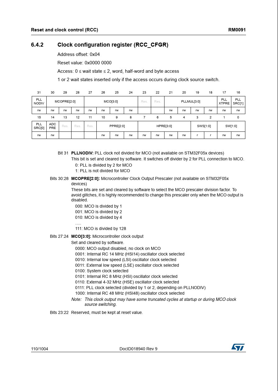
RCC_CFGR Register
We will concentrate on the RCC_CFGR register which is used to control the MCU main clock.
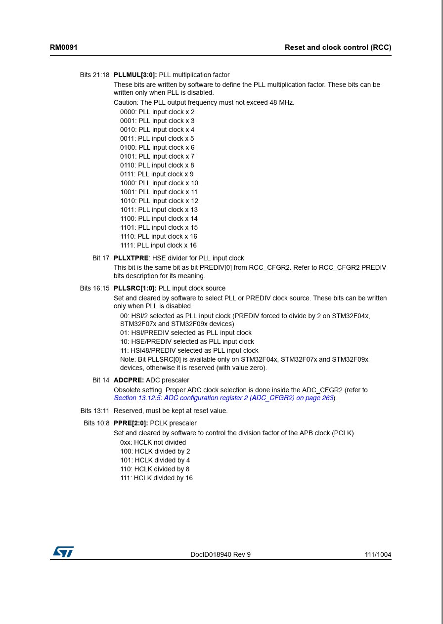
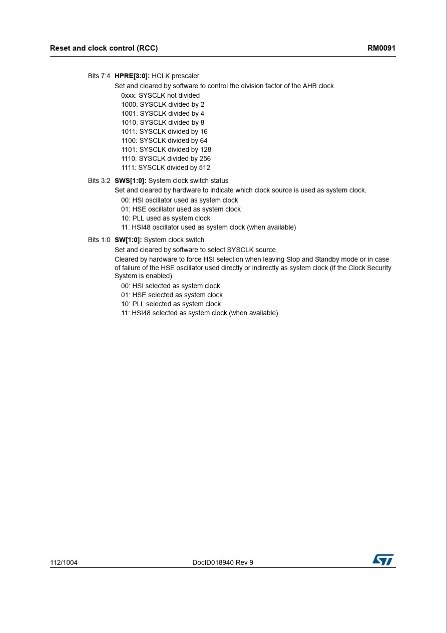
These three STMicro Reference Manual (RM0091) pages describe RCC_CFGR register operation in detail.
RCC_CFGR register page 1
RCC_CFGR register page 2
RCC_CFGR register page 3
RCC_CFGR Configuration Example
Printout of the live RCC_CFGR configuration taken from my development hardware.
RCC_CFGR.   $001D040A
                            P P P
                            L L L
                            L L L A
                            X S S D
                            T R R C
                            P C C P
       |  MCO  |   |PLLMUL |R 1 0 R|     |PPRE |
       |3:2:1:0|   |3:2:1:0|E | | E|     |2:1:0|  HPRE |SWS|SW
       |2|2|2|2|   |2|2|1|1|1|1|1|1|     |1| | |3:2:1:0|1:0|1:0
~|~|~|~|7|6|5|4|~|~|1|0|9|8|7|6|5|4|~|~|~|0|9|8|7|6|5|4|3|2|1|0
0 0 0 0 0 0 0 0 0 0 0 1 1 1 0 1 0 0 0 0 0 1 0 0 0 0 0 0 1 0 1 0
Configuration Details
Note: Only relevant bitfields are listed below.
Bitfield |
Binary Value |
Description |
|---|---|---|
SW |
10 |
PLL selected as system clock |
SWS |
10 |
PLL used as system clock |
HPRE |
0xxx |
SYSCLK not divided |
PPRE |
100 |
HCLK divided by 2 |
PLLSRC |
10 |
HSE/PREDIV selected as PLL input clock |
PLLMUL |
0111 |
PLL input clock x 9 |
MCO |
000 |
MCO is divided by 1 |
Configuration Summary
The clock (HPRE) uses the PLL with a undivided 9x multiplier. As the HPRE clock is 8 MHz multiplying by nine = 72 MHz. This MCU is being overclocked as the spec gives a maximum clock of 48 MHz for the Cortex-M0 family.
Note
I have run one unit at 96MHz for 12 months with no ill effects. I only use this for development to miniminse delays such as serial uploading. As SYSTICK is used for all timing, the source requires no changes when altering the clock speed.
Peripheral memory map
Forth
Forth Memaps and Bitfields are derived from the CMSIS-SVD and transformed by XSLT with Svd2forth.
$40021000 constant RCC             \ Reset and clock control
RCC $4 + constant RCC_CFGR (  )    \ Clock configuration register  RCC_CFGR
C Programming Language
#define PERIPH_BASE           ((uint32_t)0x40000000U)              /*!< Peripheral base address in the alias region */
#define AHBPERIPH_BASE        (PERIPH_BASE + 0x00020000)
#define RCC_BASE              (AHBPERIPH_BASE + 0x00001000)
Summary
Both systems are much the same at the peripheral memory map stage.
RCC_CFGR Bitfield Definitions
Note the Stack comments, these are my latest version and should be correct. “b” is a binary number 0|1.
Forth
\ RCC_CFGR ()
: RCC_CFGR_SW ( %bb -- x addr ) RCC_CFGR ;                 \ RCC_CFGR_SW, System clock Switch
: RCC_CFGR_SWS ( %bb -- x addr ) 2 lshift RCC_CFGR ;       \ RCC_CFGR_SWS, System Clock Switch Status
: RCC_CFGR_HPRE ( %bbbb -- x addr ) 4 lshift RCC_CFGR ;    \ RCC_CFGR_HPRE, AHB prescaler
: RCC_CFGR_PPRE ( %bbb -- x addr ) 8 lshift RCC_CFGR ;     \ RCC_CFGR_PPRE, APB Low speed prescaler  APB1
: RCC_CFGR_ADCPRE ( %bb -- x addr ) 14 lshift RCC_CFGR ;   \ RCC_CFGR_ADCPRE, ADC prescaler
: RCC_CFGR_PLLSRC ( %bb -- x addr ) 15 lshift RCC_CFGR ;   \ RCC_CFGR_PLLSRC, PLL entry clock source
: RCC_CFGR_PLLXTPRE ( -- x addr ) 17 bit RCC_CFGR ;        \ RCC_CFGR_PLLXTPRE, HSE divider for PLL entry
: RCC_CFGR_PLLMUL ( %bbbb -- x addr ) 18 lshift RCC_CFGR ; \ RCC_CFGR_PLLMUL, PLL Multiplication Factor
: RCC_CFGR_MCO ( %bbb -- x addr ) 24 lshift RCC_CFGR ;     \ RCC_CFGR_MCO, Microcontroller clock  output
Forth Configuration
To achieve the example configuration.
\ f0-disco-72mhz: Set clock to 72MHz

$40021000 constant RCC                \ Reset and clock control
RCC $0 + constant RCC_CR (  )         \ Clock control register
RCC $4 + constant RCC_CFGR (  )       \ Clock configuration register  RCC_CFGR

$40022000 constant Flash              \ When raising the Clock speed, the Flash LATENCY must be extended.
Flash $0 + constant Flash_ACR (  )    \ Flash access control register

: bit ( u -- u ) 1 swap lshift  1-foldable ;   \ turn a bit position into a binary number.

: Flash_ACR_LATENCY ( %bbb -- x addr ) Flash_ACR ;         \ Flash_ACR_LATENCY, LATENCY
: Flash_ACR_PRFTBE ( -- x addr ) 4 bit Flash_ACR ;         \ PRFTBE Prefetch buffer enable
: RCC_CR_HSEON ( -- x addr ) 16 bit RCC_CR ;               \ External High Speed clock  enable
: RCC_CR_HSERDY? ( -- 1|0 ) 17 bit RCC_CR bit@ ;           \ RCC_CR_HSERDY, External High Speed clock ready  flag
: RCC_CFGR_PLLMUL ( %bbbb -- x addr ) 18 lshift RCC_CFGR ; \ PLL Multiplication Factor
: RCC_CFGR_PLLSRC ( %bb -- x addr ) 15 lshift RCC_CFGR ;   \ PLL entry clock source
: RCC_CR_PLLON ( -- x addr ) 24 bit RCC_CR ;               \ PLL enable
: RCC_CR_PLLRDY? ( -- 1|0 ) 25 bit RCC_CR bit@ ;           \ RCC_CR_PLLRDY, PLL clock ready flag
: RCC_CFGR_SW ( %bb -- x addr ) RCC_CFGR ;                 \ System clock Switch
: RCC_CFGR_PPRE ( %bbb -- x addr ) 8 lshift RCC_CFGR ;     \ APB Low speed prescaler  APB1
: RCC_CFGR_HPRE ( %bbbb -- x addr ) 4 lshift RCC_CFGR ;    \ AHB prescaler

: f0-disco-72mhz
\ Set flash wait states to 1, turn on prefetch bit. One wait state, if 24 MHz < SYSCLK  48 MHz
%011  Flash_ACR_LATENCY bis!    \ LATENCY --> max = 1 for the stm32f0, note more latency uses less power
Flash_ACR_PRFTBE bis!

\ Enable HSE oscillator
RCC_CR_HSEON bis!
BEGIN  RCC_CR_HSERDY? UNTIL     \ Is HSE ready ?

\ Set PLL multiplication factor to 8, clock is external HSE 8MHz Xtal on Disco board.
%111 RCC_CFGR_PLLMUL bis!       \ %111: PLL input clock x 9
%10 RCC_CFGR_PLLSRC bis!        \ %10: HSE/PREDIV, 01: HSI/PREDIV

\ Enable PLL
RCC_CR_PLLON bis!
BEGIN RCC_CR_PLLRDY? UNTIL      \ Is PLL ready ?

\ Switch to PLL, set ABP and AHB Prescalers
%10 RCC_CFGR_SW bis!            \ System clock Switch: %10 PLL selected as system clock
%100  RCC_CFGR_PPRE bis!        \ APB Low speed prescaler APB1 (pclock): %100: HCLK divided by 2
;

f0-disco-72mhz
C Programming Language
Peripheral register structure
/**
  * @brief Reset and Clock Control
  */

typedef struct
{
  __IO uint32_t CR;         /*!< RCC clock control register,                    Address offset: 0x00 */
  __IO uint32_t CFGR;       /*!< RCC clock configuration register,              Address offset: 0x04 */
  __IO uint32_t CIR;        /*!< RCC clock interrupt register,                  Address offset: 0x08 */
  __IO uint32_t APB2RSTR;   /*!< RCC APB2 peripheral reset register,            Address offset: 0x0C */
  __IO uint32_t APB1RSTR;   /*!< RCC APB1 peripheral reset register,            Address offset: 0x10 */
  __IO uint32_t AHBENR;     /*!< RCC AHB peripheral clock register,             Address offset: 0x14 */
  __IO uint32_t APB2ENR;    /*!< RCC APB2 peripheral clock enable register,     Address offset: 0x18 */
  __IO uint32_t APB1ENR;    /*!< RCC APB1 peripheral clock enable register,     Address offset: 0x1C */
  __IO uint32_t BDCR;       /*!< RCC Backup domain control register,            Address offset: 0x20 */
  __IO uint32_t CSR;        /*!< RCC clock control & status register,           Address offset: 0x24 */
  __IO uint32_t AHBRSTR;    /*!< RCC AHB peripheral reset register,             Address offset: 0x28 */
  __IO uint32_t CFGR2;      /*!< RCC clock configuration register 2,            Address offset: 0x2C */
  __IO uint32_t CFGR3;      /*!< RCC clock configuration register 3,            Address offset: 0x30 */
  __IO uint32_t CR2;        /*!< RCC clock control register 2,                  Address offset: 0x34 */
} RCC_TypeDef;
Peripheral_declaration
#define RCC ((RCC_TypeDef *) RCC_BASE)
Bit Definitions
/*!< SW configuration */
#define RCC_CFGR_SW_Pos                          (0U)
#define RCC_CFGR_SW_Msk                          (0x3U << RCC_CFGR_SW_Pos)     /*!< 0x00000003 */
#define RCC_CFGR_SW                              RCC_CFGR_SW_Msk               /*!< SW[1:0] bits (System clock Switch) */
#define RCC_CFGR_SW_0                            (0x1U << RCC_CFGR_SW_Pos)     /*!< 0x00000001 */
#define RCC_CFGR_SW_1                            (0x2U << RCC_CFGR_SW_Pos)     /*!< 0x00000002 */

#define RCC_CFGR_SW_HSI                          (0x00000000U)                 /*!< HSI selected as system clock */
#define RCC_CFGR_SW_HSE                          (0x00000001U)                 /*!< HSE selected as system clock */
#define RCC_CFGR_SW_PLL                          (0x00000002U)                 /*!< PLL selected as system clock */

/*!< SWS configuration */
#define RCC_CFGR_SWS_Pos                         (2U)
#define RCC_CFGR_SWS_Msk                         (0x3U << RCC_CFGR_SWS_Pos)    /*!< 0x0000000C */
#define RCC_CFGR_SWS                             RCC_CFGR_SWS_Msk              /*!< SWS[1:0] bits (System Clock Switch Status) */
#define RCC_CFGR_SWS_0                           (0x1U << RCC_CFGR_SWS_Pos)    /*!< 0x00000004 */
#define RCC_CFGR_SWS_1                           (0x2U << RCC_CFGR_SWS_Pos)    /*!< 0x00000008 */

#define RCC_CFGR_SWS_HSI                         (0x00000000U)                 /*!< HSI oscillator used as system clock */
#define RCC_CFGR_SWS_HSE                         (0x00000004U)                 /*!< HSE oscillator used as system clock */
#define RCC_CFGR_SWS_PLL                         (0x00000008U)                 /*!< PLL used as system clock */

/*!< HPRE configuration */
#define RCC_CFGR_HPRE_Pos                        (4U)
#define RCC_CFGR_HPRE_Msk                        (0xFU << RCC_CFGR_HPRE_Pos)   /*!< 0x000000F0 */
#define RCC_CFGR_HPRE                            RCC_CFGR_HPRE_Msk             /*!< HPRE[3:0] bits (AHB prescaler) */
#define RCC_CFGR_HPRE_0                          (0x1U << RCC_CFGR_HPRE_Pos)   /*!< 0x00000010 */
#define RCC_CFGR_HPRE_1                          (0x2U << RCC_CFGR_HPRE_Pos)   /*!< 0x00000020 */
#define RCC_CFGR_HPRE_2                          (0x4U << RCC_CFGR_HPRE_Pos)   /*!< 0x00000040 */
#define RCC_CFGR_HPRE_3                          (0x8U << RCC_CFGR_HPRE_Pos)   /*!< 0x00000080 */

#define RCC_CFGR_HPRE_DIV1                       (0x00000000U)                 /*!< SYSCLK not divided */
#define RCC_CFGR_HPRE_DIV2                       (0x00000080U)                 /*!< SYSCLK divided by 2 */
#define RCC_CFGR_HPRE_DIV4                       (0x00000090U)                 /*!< SYSCLK divided by 4 */
#define RCC_CFGR_HPRE_DIV8                       (0x000000A0U)                 /*!< SYSCLK divided by 8 */
#define RCC_CFGR_HPRE_DIV16                      (0x000000B0U)                 /*!< SYSCLK divided by 16 */
#define RCC_CFGR_HPRE_DIV64                      (0x000000C0U)                 /*!< SYSCLK divided by 64 */
#define RCC_CFGR_HPRE_DIV128                     (0x000000D0U)                 /*!< SYSCLK divided by 128 */
#define RCC_CFGR_HPRE_DIV256                     (0x000000E0U)                 /*!< SYSCLK divided by 256 */
#define RCC_CFGR_HPRE_DIV512                     (0x000000F0U)                 /*!< SYSCLK divided by 512 */

/*!< PPRE configuration */
#define RCC_CFGR_PPRE_Pos                        (8U)
#define RCC_CFGR_PPRE_Msk                        (0x7U << RCC_CFGR_PPRE_Pos)   /*!< 0x00000700 */
#define RCC_CFGR_PPRE                            RCC_CFGR_PPRE_Msk             /*!< PRE[2:0] bits (APB prescaler) */
#define RCC_CFGR_PPRE_0                          (0x1U << RCC_CFGR_PPRE_Pos)   /*!< 0x00000100 */
#define RCC_CFGR_PPRE_1                          (0x2U << RCC_CFGR_PPRE_Pos)   /*!< 0x00000200 */
#define RCC_CFGR_PPRE_2                          (0x4U << RCC_CFGR_PPRE_Pos)   /*!< 0x00000400 */

#define RCC_CFGR_PPRE_DIV1                       (0x00000000U)                 /*!< HCLK not divided */
#define RCC_CFGR_PPRE_DIV2_Pos                   (10U)
#define RCC_CFGR_PPRE_DIV2_Msk                   (0x1U << RCC_CFGR_PPRE_DIV2_Pos) /*!< 0x00000400 */
#define RCC_CFGR_PPRE_DIV2                       RCC_CFGR_PPRE_DIV2_Msk        /*!< HCLK divided by 2 */
#define RCC_CFGR_PPRE_DIV4_Pos                   (8U)
#define RCC_CFGR_PPRE_DIV4_Msk                   (0x5U << RCC_CFGR_PPRE_DIV4_Pos) /*!< 0x00000500 */
#define RCC_CFGR_PPRE_DIV4                       RCC_CFGR_PPRE_DIV4_Msk        /*!< HCLK divided by 4 */
#define RCC_CFGR_PPRE_DIV8_Pos                   (9U)
#define RCC_CFGR_PPRE_DIV8_Msk                   (0x3U << RCC_CFGR_PPRE_DIV8_Pos) /*!< 0x00000600 */
#define RCC_CFGR_PPRE_DIV8                       RCC_CFGR_PPRE_DIV8_Msk        /*!< HCLK divided by 8 */
#define RCC_CFGR_PPRE_DIV16_Pos                  (8U)
#define RCC_CFGR_PPRE_DIV16_Msk                  (0x7U << RCC_CFGR_PPRE_DIV16_Pos) /*!< 0x00000700 */
#define RCC_CFGR_PPRE_DIV16                      RCC_CFGR_PPRE_DIV16_Msk       /*!< HCLK divided by 16 */

/*!< ADCPPRE configuration */
#define RCC_CFGR_ADCPRE_Pos                      (14U)
#define RCC_CFGR_ADCPRE_Msk                      (0x1U << RCC_CFGR_ADCPRE_Pos) /*!< 0x00004000 */
#define RCC_CFGR_ADCPRE                          RCC_CFGR_ADCPRE_Msk           /*!< ADCPRE bit (ADC prescaler) */

#define RCC_CFGR_ADCPRE_DIV2                     (0x00000000U)                 /*!< PCLK divided by 2 */
#define RCC_CFGR_ADCPRE_DIV4                     (0x00004000U)                 /*!< PCLK divided by 4 */

#define RCC_CFGR_PLLSRC_Pos                      (16U)
#define RCC_CFGR_PLLSRC_Msk                      (0x1U << RCC_CFGR_PLLSRC_Pos) /*!< 0x00010000 */
#define RCC_CFGR_PLLSRC                          RCC_CFGR_PLLSRC_Msk           /*!< PLL entry clock source */
#define RCC_CFGR_PLLSRC_HSI_DIV2                 (0x00000000U)                 /*!< HSI clock divided by 2 selected as PLL entry clock source */
#define RCC_CFGR_PLLSRC_HSE_PREDIV               (0x00010000U)                 /*!< HSE/PREDIV clock selected as PLL entry clock source */

#define RCC_CFGR_PLLXTPRE_Pos                    (17U)
#define RCC_CFGR_PLLXTPRE_Msk                    (0x1U << RCC_CFGR_PLLXTPRE_Pos) /*!< 0x00020000 */
#define RCC_CFGR_PLLXTPRE                        RCC_CFGR_PLLXTPRE_Msk         /*!< HSE divider for PLL entry */
#define RCC_CFGR_PLLXTPRE_HSE_PREDIV_DIV1        (0x00000000U)                 /*!< HSE/PREDIV clock not divided for PLL entry */
#define RCC_CFGR_PLLXTPRE_HSE_PREDIV_DIV2        (0x00020000U)                 /*!< HSE/PREDIV clock divided by 2 for PLL entry */

/*!< PLLMUL configuration */
#define RCC_CFGR_PLLMUL_Pos                      (18U)
#define RCC_CFGR_PLLMUL_Msk                      (0xFU << RCC_CFGR_PLLMUL_Pos) /*!< 0x003C0000 */
#define RCC_CFGR_PLLMUL                          RCC_CFGR_PLLMUL_Msk           /*!< PLLMUL[3:0] bits (PLL multiplication factor) */
#define RCC_CFGR_PLLMUL_0                        (0x1U << RCC_CFGR_PLLMUL_Pos) /*!< 0x00040000 */
#define RCC_CFGR_PLLMUL_1                        (0x2U << RCC_CFGR_PLLMUL_Pos) /*!< 0x00080000 */
#define RCC_CFGR_PLLMUL_2                        (0x4U << RCC_CFGR_PLLMUL_Pos) /*!< 0x00100000 */
#define RCC_CFGR_PLLMUL_3                        (0x8U << RCC_CFGR_PLLMUL_Pos) /*!< 0x00200000 */

#define RCC_CFGR_PLLMUL2                         (0x00000000U)                 /*!< PLL input clock*2 */
#define RCC_CFGR_PLLMUL3                         (0x00040000U)                 /*!< PLL input clock*3 */
#define RCC_CFGR_PLLMUL4                         (0x00080000U)                 /*!< PLL input clock*4 */
#define RCC_CFGR_PLLMUL5                         (0x000C0000U)                 /*!< PLL input clock*5 */
#define RCC_CFGR_PLLMUL6                         (0x00100000U)                 /*!< PLL input clock*6 */
#define RCC_CFGR_PLLMUL7                         (0x00140000U)                 /*!< PLL input clock*7 */
#define RCC_CFGR_PLLMUL8                         (0x00180000U)                 /*!< PLL input clock*8 */
#define RCC_CFGR_PLLMUL9                         (0x001C0000U)                 /*!< PLL input clock*9 */
#define RCC_CFGR_PLLMUL10                        (0x00200000U)                 /*!< PLL input clock10 */
#define RCC_CFGR_PLLMUL11                        (0x00240000U)                 /*!< PLL input clock*11 */
#define RCC_CFGR_PLLMUL12                        (0x00280000U)                 /*!< PLL input clock*12 */
#define RCC_CFGR_PLLMUL13                        (0x002C0000U)                 /*!< PLL input clock*13 */
#define RCC_CFGR_PLLMUL14                        (0x00300000U)                 /*!< PLL input clock*14 */
#define RCC_CFGR_PLLMUL15                        (0x00340000U)                 /*!< PLL input clock*15 */
#define RCC_CFGR_PLLMUL16                        (0x00380000U)                 /*!< PLL input clock*16 */
Summary
keil/Drivers/CMSIS/Device/ST/STM32F0xx/Source/Templates/system_stm32f0xx.c
Quite large differences here. C uses structures and predefines every #defined legal bitfield variation ?
Keil C Configuration
Unfortunately I couldn’t find an example config the same as mine above but this one is similar (PLL and Flash are not used) and should help to illustrate the Keil C and Forth differences regarding peripheral configuration.
This is quite long as it also caters for other slightly different models in the F0 family.
/**
******************************************************************************
* @file system_stm32f0xx.c
* @author MCD Application Team
* @brief CMSIS Cortex-M0 Device Peripheral Access Layer System Source File.
*
* 1. This file provides two functions and one global variable to be called from
* user application:
* - SystemInit(): This function is called at startup just after reset and
* before branch to main program. This call is made inside
* the "startup_stm32f0xx.s" file.
*
* - SystemCoreClock variable: Contains the core clock (HCLK), it can be used
* by the user application to setup the SysTick
* timer or configure other parameters.
*
* - SystemCoreClockUpdate(): Updates the variable SystemCoreClock and must
* be called whenever the core clock is changed
* during program execution.
*
* 2. After each device reset the HSI (8 MHz) is used as system clock source.
* Then SystemInit() function is called, in "startup_stm32f0xx.s" file, to
* configure the system clock before to branch to main program.
*
* 3. This file configures the system clock as follows:
*=============================================================================
* Supported STM32F0xx device
*-----------------------------------------------------------------------------
* System Clock source | HSI
*-----------------------------------------------------------------------------
* SYSCLK(Hz) | 8000000
*-----------------------------------------------------------------------------
* HCLK(Hz) | 8000000
*-----------------------------------------------------------------------------
* AHB Prescaler | 1
*-----------------------------------------------------------------------------
* APB1 Prescaler | 1
*-----------------------------------------------------------------------------
*=============================================================================
******************************************************************************
* @attention
*
* <h2><center>© COPYRIGHT(c) 2016 STMicroelectronics</center></h2>
*
* Redistribution and use in source and binary forms, with or without modification,
* are permitted provided that the following conditions are met:
* 1. Redistributions of source code must retain the above copyright notice,
* this list of conditions and the following disclaimer.
* 2. Redistributions in binary form must reproduce the above copyright notice,
* this list of conditions and the following disclaimer in the documentation
* and/or other materials provided with the distribution.
* 3. Neither the name of STMicroelectronics nor the names of its contributors
* may be used to endorse or promote products derived from this software
* without specific prior written permission.
*
* THIS SOFTWARE IS PROVIDED BY THE COPYRIGHT HOLDERS AND CONTRIBUTORS "AS IS"
* AND ANY EXPRESS OR IMPLIED WARRANTIES, INCLUDING, BUT NOT LIMITED TO, THE
* IMPLIED WARRANTIES OF MERCHANTABILITY AND FITNESS FOR A PARTICULAR PURPOSE ARE
* DISCLAIMED. IN NO EVENT SHALL THE COPYRIGHT HOLDER OR CONTRIBUTORS BE LIABLE
* FOR ANY DIRECT, INDIRECT, INCIDENTAL, SPECIAL, EXEMPLARY, OR CONSEQUENTIAL
* DAMAGES (INCLUDING, BUT NOT LIMITED TO, PROCUREMENT OF SUBSTITUTE GOODS OR
* SERVICES; LOSS OF USE, DATA, OR PROFITS; OR BUSINESS INTERRUPTION) HOWEVER
* CAUSED AND ON ANY THEORY OF LIABILITY, WHETHER IN CONTRACT, STRICT LIABILITY,
* OR TORT (INCLUDING NEGLIGENCE OR OTHERWISE) ARISING IN ANY WAY OUT OF THE USE
* OF THIS SOFTWARE, EVEN IF ADVISED OF THE POSSIBILITY OF SUCH DAMAGE.
*
******************************************************************************
*/
/** @addtogroup CMSIS
* @{
*/
/** @addtogroup stm32f0xx_system
* @{
*/
/** @addtogroup STM32F0xx_System_Private_Includes
* @{
*/
#include "stm32f0xx.h"
/**
* @}
*/
/** @addtogroup STM32F0xx_System_Private_TypesDefinitions
* @{
*/
/**
* @}
*/
/** @addtogroup STM32F0xx_System_Private_Defines
* @{
*/
#if !defined (HSE_VALUE)
#define HSE_VALUE ((uint32_t)8000000) /*!< Default value of the External oscillator in Hz.
This value can be provided and adapted by the user application. */
#endif /* HSE_VALUE */
#if !defined (HSI_VALUE)
#define HSI_VALUE ((uint32_t)8000000) /*!< Default value of the Internal oscillator in Hz.
This value can be provided and adapted by the user application. */
#endif /* HSI_VALUE */
#if !defined (HSI48_VALUE)
#define HSI48_VALUE ((uint32_t)48000000) /*!< Default value of the HSI48 Internal oscillator in Hz.
This value can be provided and adapted by the user application. */
#endif /* HSI48_VALUE */
/**
* @}
*/
/** @addtogroup STM32F0xx_System_Private_Macros
* @{
*/
/**
* @}
*/
/** @addtogroup STM32F0xx_System_Private_Variables
* @{
*/
/* This variable is updated in three ways:
1) by calling CMSIS function SystemCoreClockUpdate()
2) by calling HAL API function HAL_RCC_GetHCLKFreq()
3) each time HAL_RCC_ClockConfig() is called to configure the system clock frequency
Note: If you use this function to configure the system clock there is no need to
call the 2 first functions listed above, since SystemCoreClock variable is
updated automatically.
*/
uint32_t SystemCoreClock = 8000000;
const uint8_t AHBPrescTable[16] = {0, 0, 0, 0, 0, 0, 0, 0, 1, 2, 3, 4, 6, 7, 8, 9};
const uint8_t APBPrescTable[8] = {0, 0, 0, 0, 1, 2, 3, 4};
/**
* @}
*/
/** @addtogroup STM32F0xx_System_Private_FunctionPrototypes
* @{
*/
/**
* @}
*/
/** @addtogroup STM32F0xx_System_Private_Functions
* @{
*/
/**
* @brief Setup the microcontroller system.
* Initialize the default HSI clock source, vector table location and the PLL configuration is reset.
* @param None
* @retval None
*/
void SystemInit(void)
{
/* Reset the RCC clock configuration to the default reset state ------------*/
/* Set HSION bit */
RCC->CR |= (uint32_t)0x00000001U;
#if defined (STM32F051x8) || defined (STM32F058x8)
/* Reset SW[1:0], HPRE[3:0], PPRE[2:0], ADCPRE and MCOSEL[2:0] bits */
RCC->CFGR &= (uint32_t)0xF8FFB80CU;
#else
/* Reset SW[1:0], HPRE[3:0], PPRE[2:0], ADCPRE, MCOSEL[2:0], MCOPRE[2:0] and PLLNODIV bits */
RCC->CFGR &= (uint32_t)0x08FFB80CU;
#endif /* STM32F051x8 or STM32F058x8 */
/* Reset HSEON, CSSON and PLLON bits */
RCC->CR &= (uint32_t)0xFEF6FFFFU;
/* Reset HSEBYP bit */
RCC->CR &= (uint32_t)0xFFFBFFFFU;
/* Reset PLLSRC, PLLXTPRE and PLLMUL[3:0] bits */
RCC->CFGR &= (uint32_t)0xFFC0FFFFU;
/* Reset PREDIV[3:0] bits */
RCC->CFGR2 &= (uint32_t)0xFFFFFFF0U;
#if defined (STM32F072xB) || defined (STM32F078xx)
/* Reset USART2SW[1:0], USART1SW[1:0], I2C1SW, CECSW, USBSW and ADCSW bits */
RCC->CFGR3 &= (uint32_t)0xFFFCFE2CU;
#elif defined (STM32F071xB)
/* Reset USART2SW[1:0], USART1SW[1:0], I2C1SW, CECSW and ADCSW bits */
RCC->CFGR3 &= (uint32_t)0xFFFFCEACU;
#elif defined (STM32F091xC) || defined (STM32F098xx)
/* Reset USART3SW[1:0], USART2SW[1:0], USART1SW[1:0], I2C1SW, CECSW and ADCSW bits */
RCC->CFGR3 &= (uint32_t)0xFFF0FEACU;
#elif defined (STM32F030x6) || defined (STM32F030x8) || defined (STM32F031x6) || defined (STM32F038xx) || defined (STM32F030xC)
/* Reset USART1SW[1:0], I2C1SW and ADCSW bits */
RCC->CFGR3 &= (uint32_t)0xFFFFFEECU;
#elif defined (STM32F051x8) || defined (STM32F058xx)
/* Reset USART1SW[1:0], I2C1SW, CECSW and ADCSW bits */
RCC->CFGR3 &= (uint32_t)0xFFFFFEACU;
#elif defined (STM32F042x6) || defined (STM32F048xx)
/* Reset USART1SW[1:0], I2C1SW, CECSW, USBSW and ADCSW bits */
RCC->CFGR3 &= (uint32_t)0xFFFFFE2CU;
#elif defined (STM32F070x6) || defined (STM32F070xB)
/* Reset USART1SW[1:0], I2C1SW, USBSW and ADCSW bits */
RCC->CFGR3 &= (uint32_t)0xFFFFFE6CU;
/* Set default USB clock to PLLCLK, since there is no HSI48 */
RCC->CFGR3 |= (uint32_t)0x00000080U;
#else
#warning "No target selected"
#endif
/* Reset HSI14 bit */
RCC->CR2 &= (uint32_t)0xFFFFFFFEU;
/* Disable all interrupts */
RCC->CIR = 0x00000000U;
}
/**
* @brief Update SystemCoreClock variable according to Clock Register Values.
* The SystemCoreClock variable contains the core clock (HCLK), it can
* be used by the user application to setup the SysTick timer or configure
* other parameters.
*
* @note Each time the core clock (HCLK) changes, this function must be called
* to update SystemCoreClock variable value. Otherwise, any configuration
* based on this variable will be incorrect.
*
* @note - The system frequency computed by this function is not the real
* frequency in the chip. It is calculated based on the predefined
* constant and the selected clock source:
*
* - If SYSCLK source is HSI, SystemCoreClock will contain the HSI_VALUE(*)
*
* - If SYSCLK source is HSE, SystemCoreClock will contain the HSE_VALUE(**)
*
* - If SYSCLK source is PLL, SystemCoreClock will contain the HSE_VALUE(**)
* or HSI_VALUE(*) multiplied/divided by the PLL factors.
*
* (*) HSI_VALUE is a constant defined in stm32f0xx_hal.h file (default value
* 8 MHz) but the real value may vary depending on the variations
* in voltage and temperature.
*
* (**) HSE_VALUE is a constant defined in stm32f0xx_hal.h file (default value
* 8 MHz), user has to ensure that HSE_VALUE is same as the real
* frequency of the crystal used. Otherwise, this function may
* have wrong result.
*
* - The result of this function could be not correct when using fractional
* value for HSE crystal.
*
* @param None
* @retval None
*/
void SystemCoreClockUpdate (void)
{
uint32_t tmp = 0, pllmull = 0, pllsource = 0, predivfactor = 0;
/* Get SYSCLK source -------------------------------------------------------*/
tmp = RCC->CFGR & RCC_CFGR_SWS;
switch (tmp)
{
case RCC_CFGR_SWS_HSI: /* HSI used as system clock */
SystemCoreClock = HSI_VALUE;
break;
case RCC_CFGR_SWS_HSE: /* HSE used as system clock */
SystemCoreClock = HSE_VALUE;
break;
case RCC_CFGR_SWS_PLL: /* PLL used as system clock */
/* Get PLL clock source and multiplication factor ----------------------*/
pllmull = RCC->CFGR & RCC_CFGR_PLLMUL;
pllsource = RCC->CFGR & RCC_CFGR_PLLSRC;
pllmull = ( pllmull >> 18) + 2;
predivfactor = (RCC->CFGR2 & RCC_CFGR2_PREDIV) + 1;
if (pllsource == RCC_CFGR_PLLSRC_HSE_PREDIV)
{
/* HSE used as PLL clock source : SystemCoreClock = HSE/PREDIV * PLLMUL */
SystemCoreClock = (HSE_VALUE/predivfactor) * pllmull;
}
#if defined(STM32F042x6) || defined(STM32F048xx) || defined(STM32F072xB) || defined(STM32F078xx) || defined(STM32F091xC) || defined(STM32F098xx)
else if (pllsource == RCC_CFGR_PLLSRC_HSI48_PREDIV)
{
/* HSI48 used as PLL clock source : SystemCoreClock = HSI48/PREDIV * PLLMUL */
SystemCoreClock = (HSI48_VALUE/predivfactor) * pllmull;
}
#endif /* STM32F042x6 || STM32F048xx || STM32F072xB || STM32F078xx || STM32F091xC || STM32F098xx */
else
{
#if defined(STM32F042x6) || defined(STM32F048xx) || defined(STM32F070x6) \
|| defined(STM32F078xx) || defined(STM32F071xB) || defined(STM32F072xB) \
|| defined(STM32F070xB) || defined(STM32F091xC) || defined(STM32F098xx) || defined(STM32F030xC)
/* HSI used as PLL clock source : SystemCoreClock = HSI/PREDIV * PLLMUL */
SystemCoreClock = (HSI_VALUE/predivfactor) * pllmull;
#else
/* HSI used as PLL clock source : SystemCoreClock = HSI/2 * PLLMUL */
SystemCoreClock = (HSI_VALUE >> 1) * pllmull;
#endif /* STM32F042x6 || STM32F048xx || STM32F070x6 ||
STM32F071xB || STM32F072xB || STM32F078xx || STM32F070xB ||
STM32F091xC || STM32F098xx || STM32F030xC */
}
break;
default: /* HSI used as system clock */
SystemCoreClock = HSI_VALUE;
break;
}
/* Compute HCLK clock frequency ----------------*/
/* Get HCLK prescaler */
tmp = AHBPrescTable[((RCC->CFGR & RCC_CFGR_HPRE) >> 4)];
/* HCLK clock frequency */
SystemCoreClock >>= tmp;
}
/**
* @}
*/
/**
* @}
*/
/**
* @}
*/
/************************ (C) COPYRIGHT STMicroelectronics *****END OF FILE****/