Svd2forth-v3
Because Forth is interactive, the contents of all MCU Registers can be written or read in real time at the terminal. This feature is quite unique and the main reason that Forth is so productive during development.
Other systems such as C require GDB via SWD or JTAG, or a serial debugger working through a bootloader to enable the developer to see and change Register contents in real time.
However for a complex MCU such as the STM32F there are literally hundreds or thousands of Registers making easy reading of their contents a exercise in databook study and interpretation. Sure, a good designer has to know the databook intimately anyway, but fast and easy Peripheral/Register/Bitfield reading saves a lot of time and is what Svd2forth-v3 is all about.
Plus if you are new to STM32F, then Svd2forth-v3 may help reduce the inevitable information overload you will encounter.
Svd2forth-v3 takes a CMSIS-SVD file created by STM and from it automatically creates memory-mapped Register, Register Bitfield and Pretty Printing Words.
Svd2forth-v3 Peripheral Register Pretty Printing
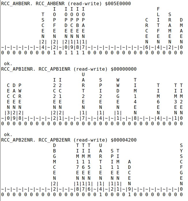
This screenpic shows a partial RCC Peripheral printout after entering “rcc.” The top third shows the RCC_ABHENR register configuration right now and it is obvious that IOP (GPIO) A,B,C,D,and F have been enabled by the “1” in the bottom line under each Bitfield.
Conversely, DMAEN is NOT enabled as it is configured to “0”.
The lowest third of this picture, RCC_APB2ENR shows that UART1 is enabled (UART1EN), as is the ADC (ADCEN) however they are the only ones.
Svd2forth-v3 differs from V2 in the following ways
? |
Differences |
|---|---|
1 |
Register Legends can be hand made to enable fast interpretation of real time contents |
2 |
Pretty Printing Legends are separated from the XML file and now contained in a “fxxx-legends.fs” file. This will allow different MCU Legend files to be created. |
3 |
There is no “Register-Reference” file, it has been replaced with “bitfields.fs” |
4 |
Both bitfields.fs and memmap.fs include the ‘description’ field from the SVD. Hopefully this will reduce the need to have a databook open while coding. |
These notes
Are specifically for a STM32F051 but will work with any other STM32Fxx with the correct SVD file, however the Register ‘Pretty Printing’ Legends (f051-legends.fs) are for a STM32F051. This can be modified for your MCU, email me if you need more information.
Howto
Untar svd2forth-v3 to a directory and in it:
Edit the Makefile and replace the STM32F0xx-tp1.svd named in “FOLDED_SVD” with the SVD FILE for the MCU you are using.
run “make everything”, this creates template.xml, bitfields.fs, and memmap.fs
Edit “template.xml” and COMMENT OUT the Peripherals you are NOT using
Commented out ? |
|
|---|---|
No |
<name xmlns:xs=”http://www.w3.org/2001/XMLSchema-instance”>GPIOE</name> |
Yes |
<!– <name xmlns:xs=”http://www.w3.org/2001/XMLSchema-instance”>GPIOE</name> –> |
- run “make”
This will create new bitfields.fs and memmap.fs based on your edited template.xml file.
Upload f051-legends.fs then memmap.fs to your MCU. If the Flash or Ram is filled, then perhaps you didn’t bother editing template.xml to reduce the size ?
bitfields.fs are for copy and pasting into your Forth program to configure Register Bitfields.
Printing a Peripheral
For every Peripheral enabled in template.xml there will be Pretty Print words generated in memmap.fs. Some will have handmade custom Legends but most will have a default format. Assume GPIOA is enabled in template.xml.
Enter “gpioa.” into your terminal, note the PERIOD after the Peripheral name, this is the “print Peripheral” command.
Note
Bitfields are grouped according to the STM Reference Manual, some are one bit groups, such as GPIOA_OTYPER, others are two bit groupings such as GPIOA_MODER, or four bit groupings as in GPIOA_AFRL. The GPIOx grouping have been hand edited otherwise automatic grouping of one bit groups applies.
gpioa.
gpioa. GPIOA_MODER (read-write) $02A80000
15|14|13|12|11|10|09|08|07|06|05|04|03|02|01|00
00 00 00 10 10 10 10 00 00 00 00 00 00 00 00 00

GPIOA_OTYPER (read-write) $00000000
1|1|1|1|1|1|
5|4|3|2|1|0|9|8|7|6|5|4|3|2|1|0
0 0 0 0 0 0 0 0 0 0 0 0 0 0 0 0

GPIOA_OSPEEDR (read-write) $0C000000
15|14|13|12|11|10|09|08|07|06|05|04|03|02|01|00
00 00 11 00 00 00 00 00 00 00 00 00 00 00 00 00

GPIOA_PUPDR (read-write) $24000000
15|14|13|12|11|10|09|08|07|06|05|04|03|02|01|00
00 10 01 00 00 00 00 00 00 00 00 00 00 00 00 00

GPIOA_IDR (read-only) $0000A5FA
1|1|1|1|1|1|
5|4|3|2|1|0|9|8|7|6|5|4|3|2|1|0
1 0 1 0 0 1 1 1 1 1 1 1 1 0 1 0

GPIOA_ODR (read-write) $00000000
1|1|1|1|1|1|
5|4|3|2|1|0|9|8|7|6|5|4|3|2|1|0
0 0 0 0 0 0 0 0 0 0 0 0 0 0 0 0

GPIOA_BSRR (write-only) $00000000
3|3|2|2|2|2|2|2|2|2|2|2|1|1|1|1|1|1|1|1|1|1|
1|0|9|8|7|6|5|4|3|2|1|0|9|8|7|6|5|4|3|2|1|0|9|8|7|6|5|4|3|2|1|0
0 0 0 0 0 0 0 0 0 0 0 0 0 0 0 0 0 0 0 0 0 0 0 0 0 0 0 0 0 0 0 0

GPIOA_LCKR (read-write) $00000000
3|3|2|2|2|2|2|2|2|2|2|2|1|1|1|1|1|1|1|1|1|1|
1|0|9|8|7|6|5|4|3|2|1|0|9|8|7|6|5|4|3|2|1|0|9|8|7|6|5|4|3|2|1|0
0 0 0 0 0 0 0 0 0 0 0 0 0 0 0 0 0 0 0 0 0 0 0 0 0 0 0 0 0 0 0 0

GPIOA_AFRL (read-write) $00000000
 07   06   05   04   03   02   01   00
0000 0000 0000 0000 0000 0000 0000 0000

GPIOA_AFRH (read-write) $00011110
 15   14   13   12   11   10   09   08
0000 0000 0000 0001 0001 0001 0001 0000

GPIOA_BRR (write-only) $00000000
1|1|1|1|1|1|
5|4|3|2|1|0|9|8|7|6|5|4|3|2|1|0
0 0 0 0 0 0 0 0 0 0 0 0 0 0 0 0

ok.
Printing a Register
Registers can be printed individually. Enter “GPIOA_IDR.” into your terminal, note the PERIOD after the Register name, this is the “print Register” command.
GPIOA_IDR.
GPIOA_ODR. GPIOA_ODR (read-write) $00000000
1|1|1|1|1|1|
5|4|3|2|1|0|9|8|7|6|5|4|3|2|1|0
0 0 0 0 0 0 0 0 0 0 0 0 0 0 0 0

ok.
Using bitfields.fs in your code
There are two types of Bitfields generated:
ONE configuration bit only, i.e.
: GPIOF_OTYPER_OT15 %1 15 lshift GPIOF_OTYPER bi? ; \ GPIOF_OTYPER_OT15 Port x configuration bit 15
This type of bitfield will usually SET or CLEAR the one bit with a “bis!” or “bic!” command, or it may possibly be tested with a “bit@” command. See the Dictionary for more information.
More than one configuration bit, i.e.
: GPIOF_MODER_MODER15 ( %XX -- ) 30 lshift GPIOF_MODER bis! ; \ GPIOF_MODER_MODER15 Port x configuration bits y = 0..15
I’ve selected code readability over size, so I usually use multiple bit Bitfields (in combination with the above command) this way:
: GPIOF_MODER_MODER15   ( %XX -- ) 30 lshift GPIOF_MODER bis! ;  \ GPIOF_MODER_MODER15    Port x configuration bits y =  0..15
%01 GPIOF_MODER_MODER15                                          \ set GPIOF-15 as a OUTPUT
RCC Memmap.fs Example
This shows the contents of the RCC Peripheral section in memmap.fs. This is the file where Peripherals and Registers are memory mapped to the hardware, a bit like a C header file. It is also the file where Pretty Printing Words are created. This file is referenced by the Words in bitfields.fs and it references the Words in fxxx-legends.fs.
$40021000 constant RCC ( Reset and clock control )
RCC $0 + constant RCC_CR ( Clock control register )
RCC $4 + constant RCC_CFGR ( Clock configuration register  RCC_CFGR )
RCC $8 + constant RCC_CIR ( Clock interrupt register  RCC_CIR )
RCC $C + constant RCC_APB2RSTR ( APB2 peripheral reset register  RCC_APB2RSTR )
RCC $10 + constant RCC_APB1RSTR ( APB1 peripheral reset register  RCC_APB1RSTR )
RCC $14 + constant RCC_AHBENR ( AHB Peripheral Clock enable register  RCC_AHBENR )
RCC $18 + constant RCC_APB2ENR ( APB2 peripheral clock enable register  RCC_APB2ENR )
RCC $1C + constant RCC_APB1ENR ( APB1 peripheral clock enable register  RCC_APB1ENR )
RCC $20 + constant RCC_BDCR ( Backup domain control register  RCC_BDCR )
RCC $24 + constant RCC_CSR ( Control/status register  RCC_CSR )
RCC $28 + constant RCC_AHBRSTR ( AHB peripheral reset register )
RCC $2C + constant RCC_CFGR2 ( Clock configuration register 2 )
RCC $30 + constant RCC_CFGR3 ( Clock configuration register 3 )
RCC $34 + constant RCC_CR2 ( Clock control register 2 )
: RCC_CR. ." RCC_CR () $" RCC_CR @ hex. RCC_CR RCC_CR.. ;
: RCC_CFGR. ." RCC_CFGR () $" RCC_CFGR @ hex. RCC_CFGR RCC_CFGR.. ;
: RCC_CIR. ." RCC_CIR () $" RCC_CIR @ hex. RCC_CIR 1b. ;
: RCC_APB2RSTR. ." RCC_APB2RSTR (read-write) $" RCC_APB2RSTR @ hex. RCC_APB2RSTR 1b. ;
: RCC_APB1RSTR. ." RCC_APB1RSTR (read-write) $" RCC_APB1RSTR @ hex. RCC_APB1RSTR 1b. ;
: RCC_AHBENR. ." RCC_AHBENR (read-write) $" RCC_AHBENR @ hex. RCC_AHBENR RCC_AHBENR.. ;
: RCC_APB2ENR. ." RCC_APB2ENR (read-write) $" RCC_APB2ENR @ hex. RCC_APB2ENR RCC_APB2ENR.. ;
: RCC_APB1ENR. ." RCC_APB1ENR (read-write) $" RCC_APB1ENR @ hex. RCC_APB1ENR RCC_APB1ENR.. ;
: RCC_BDCR. ." RCC_BDCR () $" RCC_BDCR @ hex. RCC_BDCR 1b. ;
: RCC_CSR. ." RCC_CSR () $" RCC_CSR @ hex. RCC_CSR RCC_CSR.. ;
: RCC_AHBRSTR. ." RCC_AHBRSTR (read-write) $" RCC_AHBRSTR @ hex. RCC_AHBRSTR 15b. ;
: RCC_CFGR2. ." RCC_CFGR2 (read-write) $" RCC_CFGR2 @ hex. RCC_CFGR2 RCC_CFGR2.. ;
: RCC_CFGR3. ." RCC_CFGR3 (read-write) $" RCC_CFGR3 @ hex. RCC_CFGR3 RCC_CFGR3.. ;
: RCC_CR2. ." RCC_CR2 () $" RCC_CR2 @ hex. RCC_CR2 RCC_CR2.. ;
: RCC.
RCC_CR.
RCC_CFGR.
RCC_CIR.
RCC_APB2RSTR.
RCC_APB1RSTR.
RCC_AHBENR.
RCC_APB2ENR.
RCC_APB1ENR.
RCC_BDCR.
RCC_CSR.
RCC_AHBRSTR.
RCC_CFGR2.
RCC_CFGR3.
RCC_CR2.
;
RCC_CR2 bitfields.fs Example
Note
Replace ‘bi?’ with ‘bit@’ to test bit, ‘bis!’ to SET bit, ‘bic!’ to CLEAR bit etc.
\ RCC_CR2 ()
: RCC_CR2_HSI14ON    %1 0 lshift RCC_CR2 bi? ;                 \ RCC_CR2_HSI14ON    HSI14 clock enable
: RCC_CR2_HSI14RDY   %1 1 lshift RCC_CR2 bi? ;                 \ RCC_CR2_HSI14RDY    HR14 clock ready flag
: RCC_CR2_HSI14DIS   %1 2 lshift RCC_CR2 bi? ;                 \ RCC_CR2_HSI14DIS    HSI14 clock request from ADC  disable
: RCC_CR2_HSI14TRIM   ( %XXXXX -- ) 3 lshift RCC_CR2 bi? ;     \ RCC_CR2_HSI14TRIM    HSI14 clock trimming
: RCC_CR2_HSI14CAL    ( %XXXXXXXX -- ) 8 lshift RCC_CR2 bi? ;  \ RCC_CR2_HSI14CAL    HSI14 clock calibration
RCC_CR2 Pretty Print Example
This example shows hand edited Legends using the syntax of the STM Reference Manual.
rcc_cr2.
RCC_CR2 () $00006780

                                                          H H
                                                          S S H
                                                          I I S
                                                          1 1 I
                                                          4 4 1
                               |HSICAL         |HSI14    |D R 4
                               |7:6:5:4:3:2:1:0|TRIM     |I|D|O
                               |1|1|1|1|1|1|   |4:3:2:1:0|S|Y|N
~|~|~|~|~|~|~|~|~|~|~|~|~|~|~|~|5|4|3|2|1|0|9|8|7|6|5|4|3|2|1|0
0 0 0 0 0 0 0 0 0 0 0 0 0 0 0 0 0 1 1 0 0 1 1 1 1 0 0 0 0 0 0 0