Pcb-rnd
To make Forth devices, one needs a great Open Source PCB CAD program and my choice in 2022 is PCB-RND by Tibor ‘Igor2’ Palinkas and team.
PCB-RND is a rewrite of my favorite PCB CAD of all time, PCB started by Thomas Nau in 1990.
This is a quick preview. so if you need a great GPL PCB cad, you can check it out yourself at THIS LINK.
PCB-RND is probably in your Unix repo ready to download anyway.
Workflow
Pcb-rnd uses what I call the ‘traditional pcb workflow’ in that a design proceeds in the following stages:
A schematic is designed using a schematic capture program. I happen to use gSchem because I find it so similar to ORCAD for DOS and gSchem has the easiest parts library creation.
A netlist is created to transfer the information from the schematic capture program using Gnetlist
A PCB CAD then inputs the netlist (which contains the part and connection information), allowing part placement and rubberbanding. Backannotation is also important so that changes to the PCB are reflected back to the netlist. Back in the old days, this was done via a automatically generated ECO or engineering change order. A netlist allows disparate software types to interwork together so you’re not stuck with the Schematic Capture you hate, just to use a PCB CAD you love.
Optional but highly recommended. Fossil SCM. All the gEDA formats are TEXT files, perfect for a Revision Control System because they don’t have binary blobs in proprietary formats. This allows all kinds of handy features, such as comparing the differences between schematic/pcb versions etc.
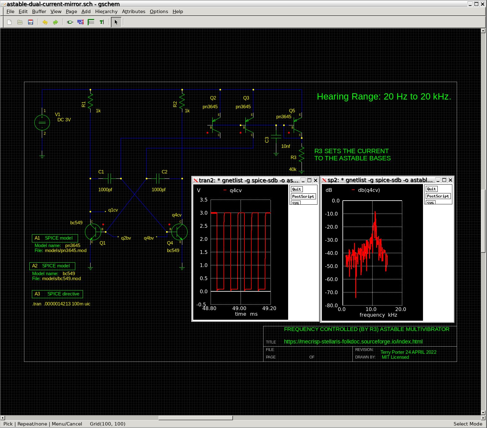
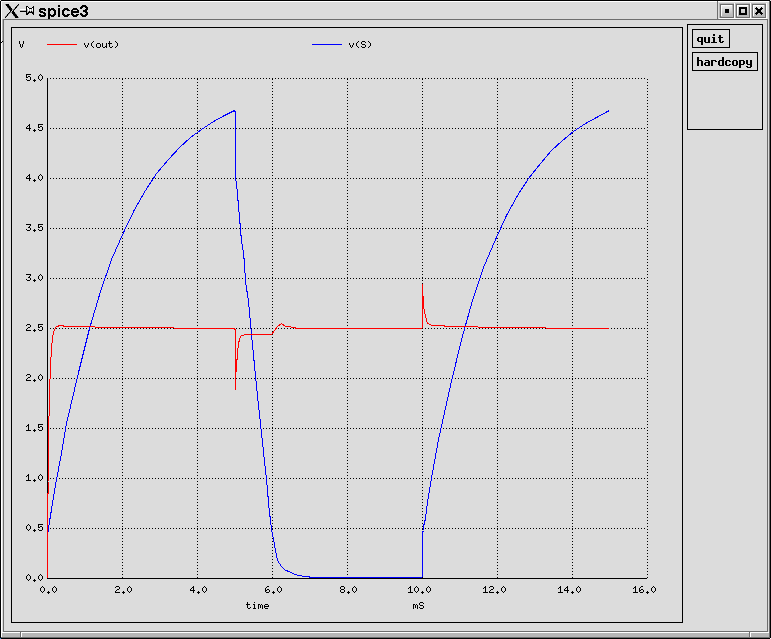
Spice
The generation of a netlist allows the schematic to be imported into other applications, your choice of analog or digital SPICE etc.
Monoliths
Modern trends tend to incorporate the schematic capture and PCB CAD into the one program, examples are Kicad etc. I can’t speak to their utility as I don’t use them but they look seriously capable and up to date with all kinds of bling.
PCB Fabs
The super cheap Fab JLCPCB makes available a Cloud hosted commercial easyEDA PCB CAD that has their parts supplier branch integrated so you can do everything on your browser including having your pcb assembled before it’s shipped to you.
I personally would never commit my designs to the cloud for dozens of reasons, but it is undeniably convenient.
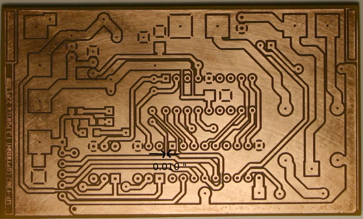
Example PCB
I made this pcb at home in 1999, using PCB. It was made using a laser printer to make a photo mask and then exposed in a light box before being etched in a small plastic tray.
The picture was taken about 10 - 15 years later when the copper was very green and corroded. After a quick hand sand with some wet and dry sandpaper this pic was taken.
I still have it because it was a mod of a existing product and I messed up the SMT transistor footprints.
Warning
This is a board that I designed 23 years ago and I can still use the design files in GPL software I compiled last week. Will the latest Java loaded proprietary CAD that is so convienent to use in a browser allow you to review your work in a quarter century ? Will you be able to show your kids or your grandkids what you made back then, or will your creative history be forever beyond reach ?
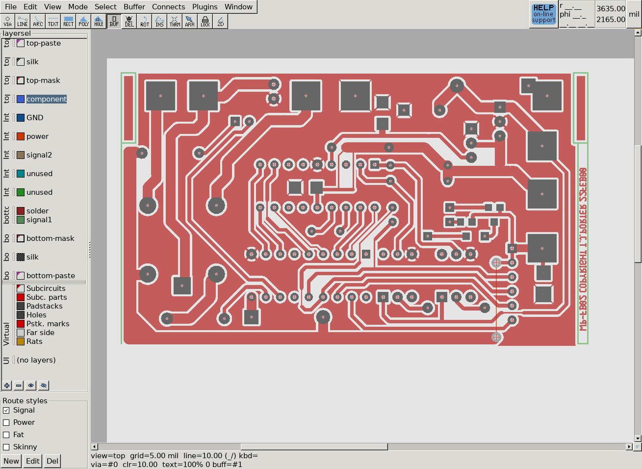
Pcb-rnd Gui
Loading my original 1999 design file with no changes.
Warning
Don’t be fooled by the simple looking GUI because underneath this careful ergonomic layout lurks MASSIVE capability and complexity. For instance intense full time development started on PCB-RND in 2015.
P.S. I’m planing a JLC-PCB made pcb using my new DSBGA chip with PCB-RND and will add that project to this doc site when it’s done.
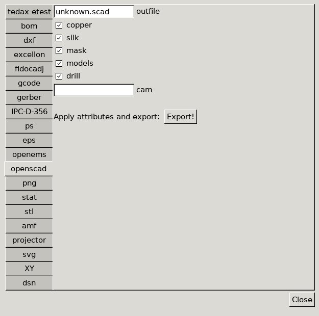
Export Formats
PCB-RND exports to all kinds of formats.
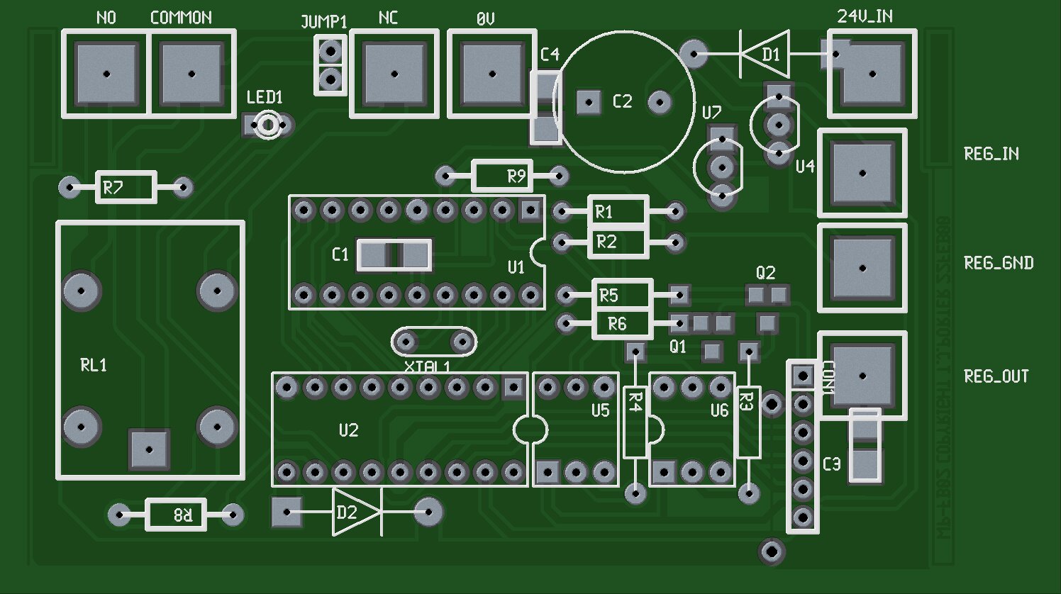
png
This provides a handy xray view of the board for development and later construction.
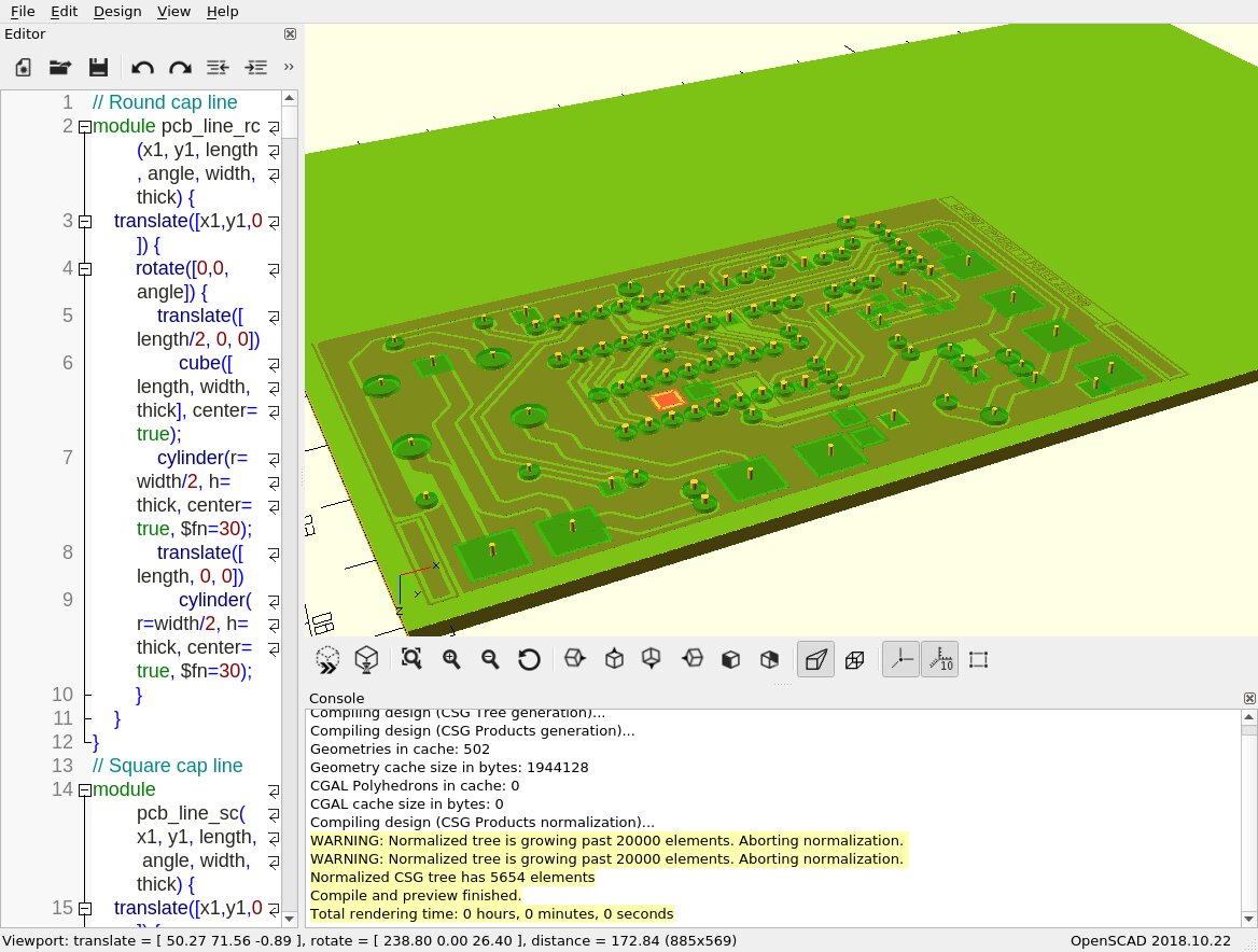
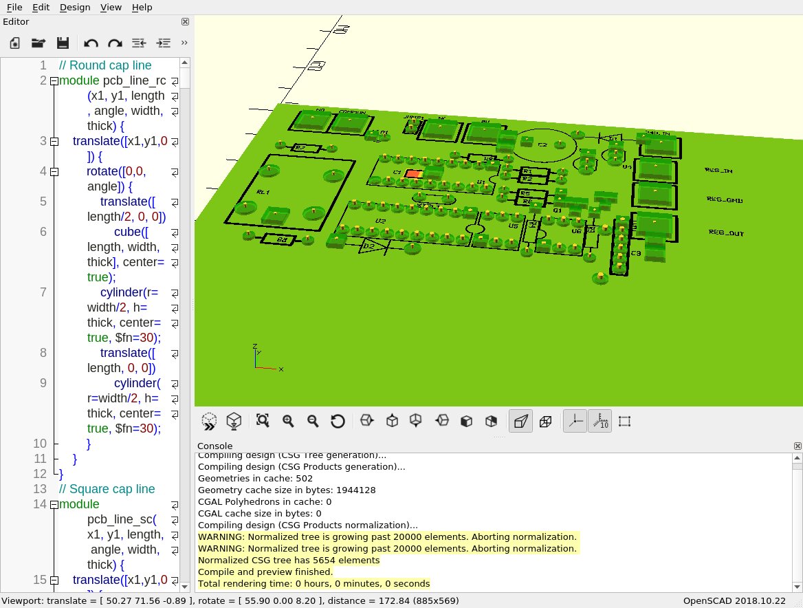
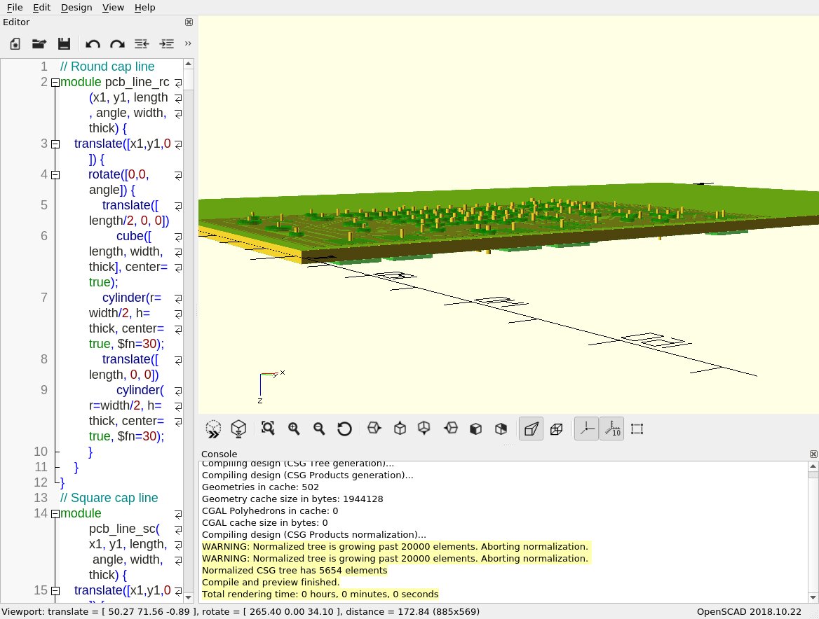
Openscad
These views are the same file just rotated and flipped etc. The parts are not in 3D because they do not contain that information for PCB-RND to export, having come from 1999. Modern parts would have that information I imagine.
This facility may also allow one to create a 3D printer enclosure with lid etc, and to try the actual pcb part in that enclosure for fit and mountings before actually printing anything ?
Copper View
Component View
Side view
Summary
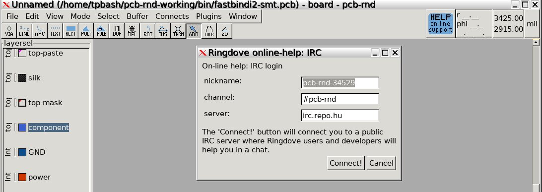
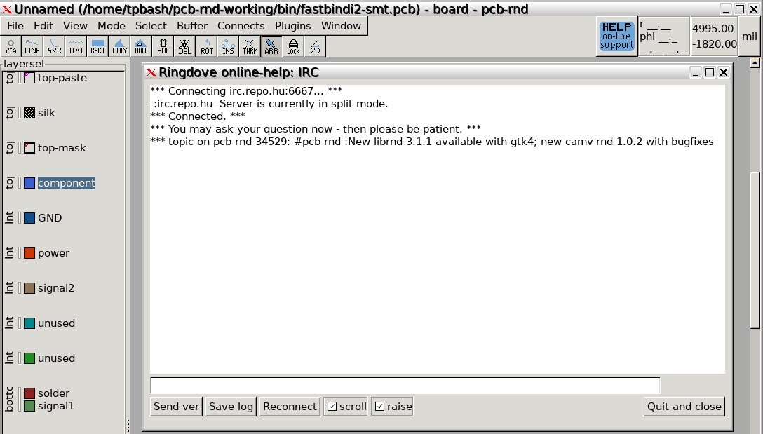
I hope I have enticed you to try PCB-RND and if you have any issues while using it, just click on the BLUE BUTTON which I think is a unique concept which connects you in realtime to the PCB-RND IRC server where you can chat to the designers, maintainers and users.
This is seriously good REAL TIME HELP folks.
The Blue HELP Button

IRC Connect Menu
Talking to the Helpline
My personal gratitude to Tibor and team for reincarnating the stagnant PCB with a much improved PCB-RND