Prototyping
General descriptions of the methods I use for prototyping small Forth powered devices. Prototyping is usually limited to one or two units, and if a prototype was going to go into production, I would use a commercially made run of PCB’s instead.
Normally, a prototype and production unit have very little in common.
See also
Hardware
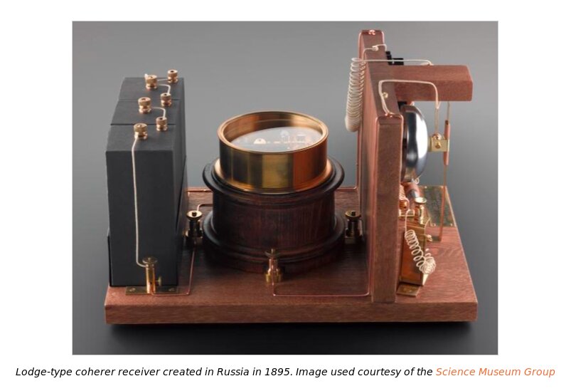
A beautiful example of prototyping to inspire us all, a Lodge ‘Coherer’ hand made in Russia in 1895.
Wiring
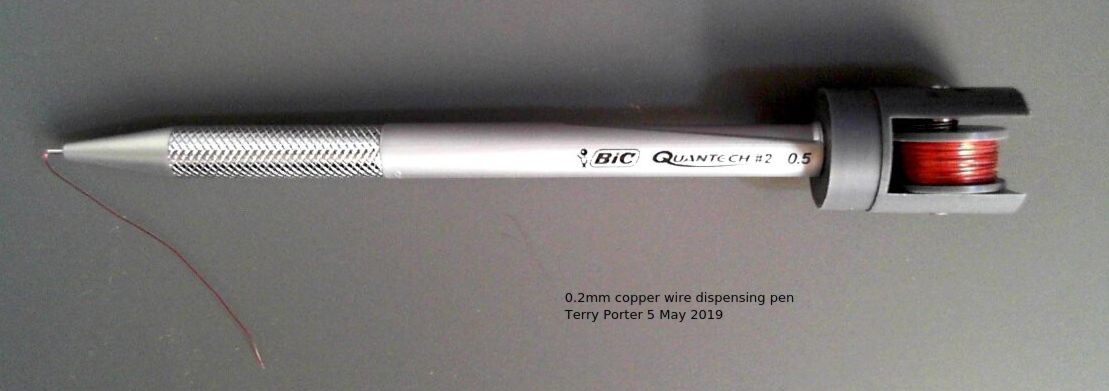
My home made wiring pen spooled with 32 AWG or 0.2 mm enameled wire.
Wiring Pen
For analog and digital signal prototype wiring I hand-wire using 0.2mm enameled copper wire (also called “magnet wire”) with the dispensing pen in the picture above. This was a off-the-shelf 0.5mm BiC lead pencil fitted with a bobbin/frame I machined out of PVC. In the gap between bobbin and frame is a small spring providing the friction necessary to prevent the bobbin spinning and un-spooling the wire by accident.
The magnet wire is coated with enamel which is easily removed by sliding a blob of solder on the tip of a soldering iron over the end of the wire. Unlike 0.22mm plastic coated wire wrap wire the enamel removal is clean and tidy without having to scrape of melted plastic afterwards. The enameled copper wire also holds its shape where the alternative is slightly springy and much bulkier.
Note
Insulation removal other than at the end of the wire is difficult and I don’t generally do that, rather I use point to point wiring rather than a continuous string when connecting a number of pins together.
Wire Source
I use the wire from a old transformer winding, old electromagnet loudspeaker wire is also a great source. If buying online, check the temperature rating of the insulation which should be 180C or less if possible. If it isn’t then the wire won’t be suitable, and if the vendor doesn’t know, search elsewhere.
Source of suitable wire
Company |
Insulation melt temp |
Sizes (mm) |
Comments |
|---|---|---|---|
Remington Industries |
105°C |
lots |
Plain Enamel/Formvar, ~$8 USD and up dep on weight |
Scientific Wire |
155 - 180 C |
0.180 - 1.25 |
green, red, and orange, 6kg minimum £66 + shipping |
https://www.remingtonindustries.com/magnet-wire/magnet-wire-by-awg/
https://www.scientificwire.com/acatalog/ec-wire.html
Iron Temperature
350C of soldering temperature is recommended for this process.
Visual Difference Between Suitable and Unsuitable Wire ?
None, they all look alike.
REASONS FOR FAILURE
Iron tip not hot enough
Wire insulation is wrong type. These days it’s difficult to ensure the parts you buy are what the vendor claims them to be. If this method didn’t work, I wouldn’t have been using it since 1976 and writing about it here.
Trying to remove insulation in middle of wire and not at the end
Examples
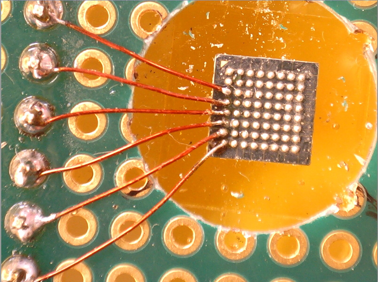
My Work
Wire was spooled via my ‘wiring pen’ above and hand soldered. This project is unfinished at the time of the picture.
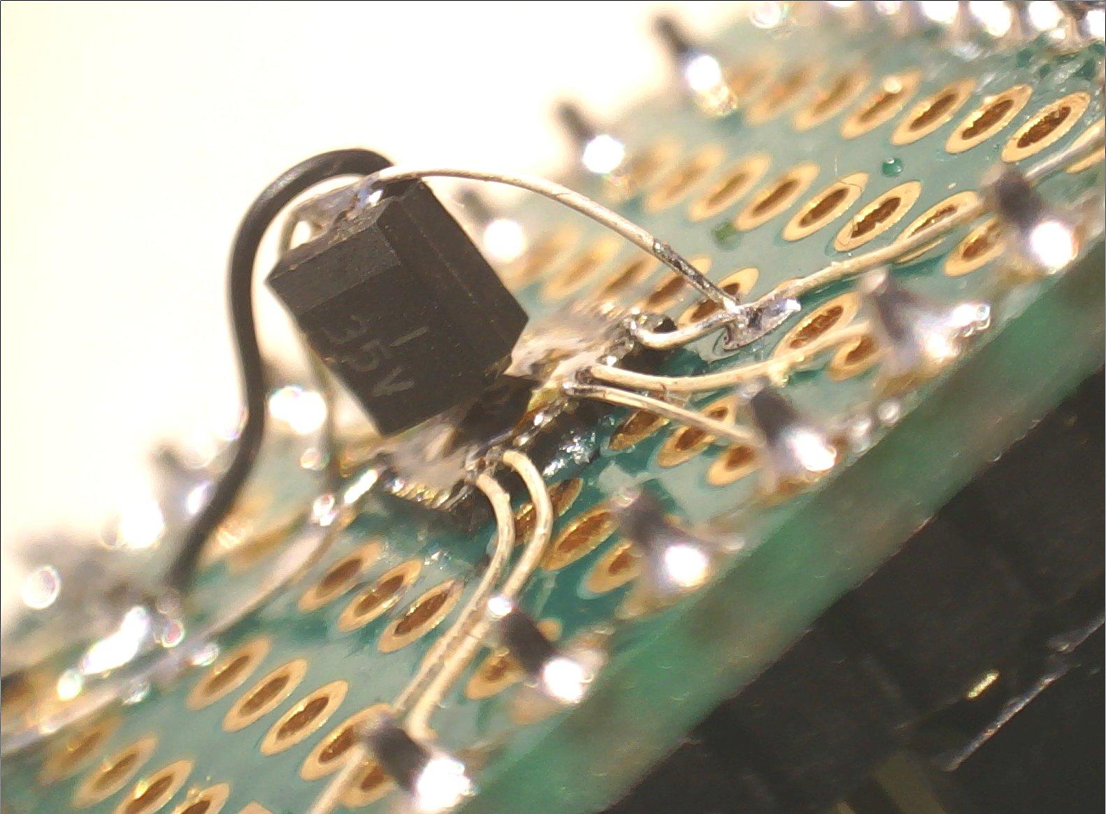
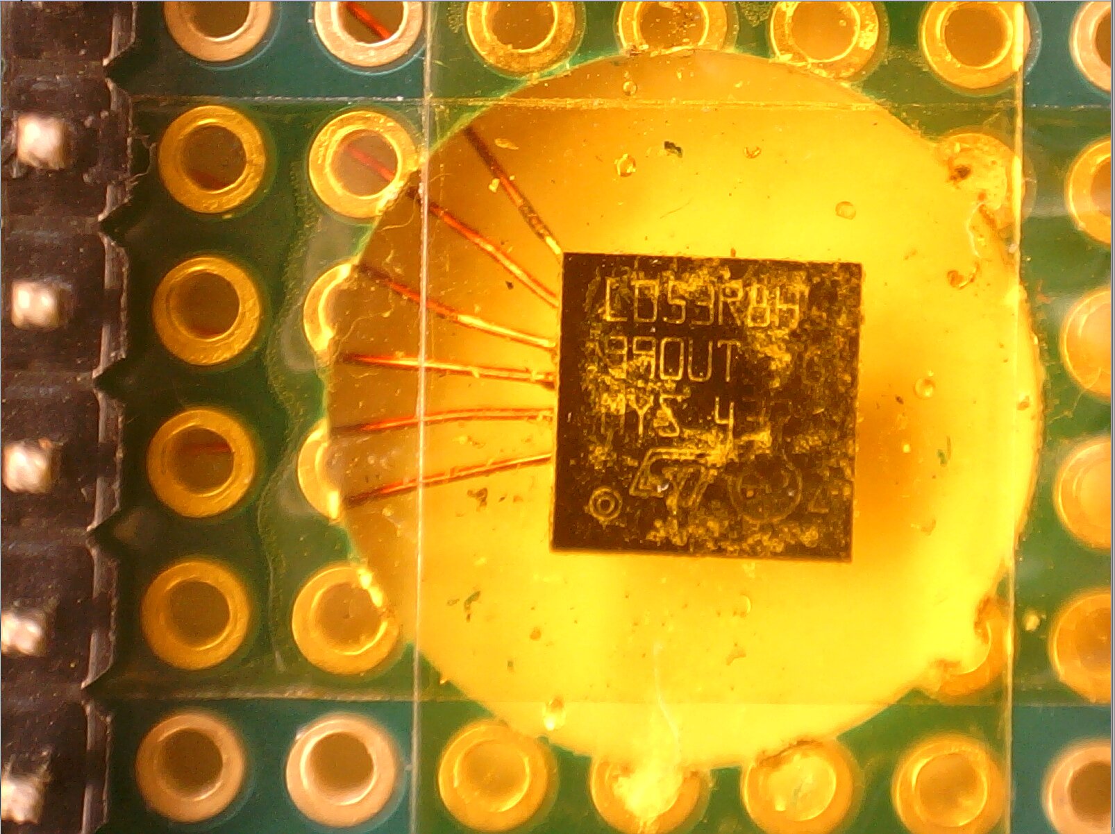
STM32L053
material: 0.1” pitch matrix board from a STM32 Discovery Board Kit
Wire: 0.2mm polyurethane enameled copper wire which is the smallest I have.
Hole drilled board for SMT chip
Kapton tape used to retain the chip in hole
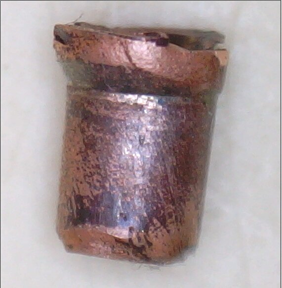
Copper Rivets
I’m experimenting with home made, hand operated, tool formed, copper rivets to use with BGA and QFN MCU’s, hand spooled wire, blank Teflon pcb, Kapton tape and hand soldering.
These are some pictures of my third prototype rivet. It is approximately 4mm by 2.3mm in size and made from solid copper wire recovered from a old transformer.
The rivets will be used as smt, leaded components and multicore wire anchor/solder points, with some rivets being drilled thru like a via on a etched pcb.
Note
All pics are from a USB microscope.
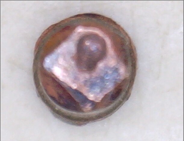
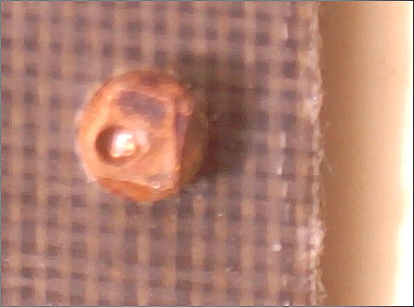
Rivet side view: the shaft is 2.3 mm in diameter
This image is 30.5 times larger than life size.
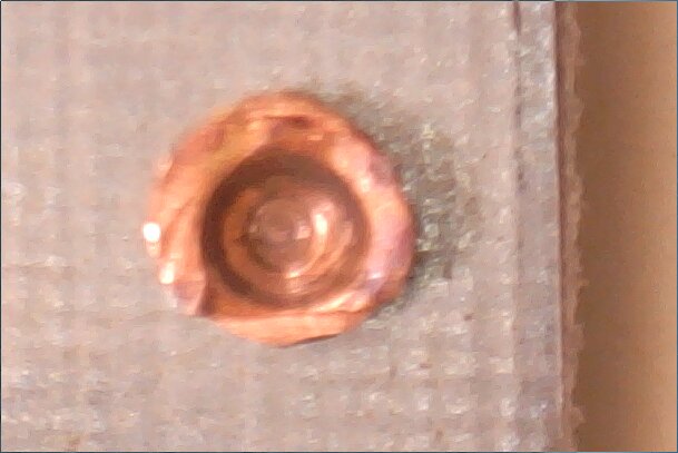
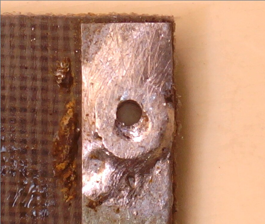
Rivet top view
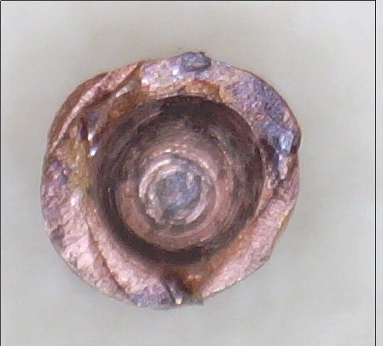
Rivet focus bottom of top lip
Rivets next to 2.3mm hole in PCB
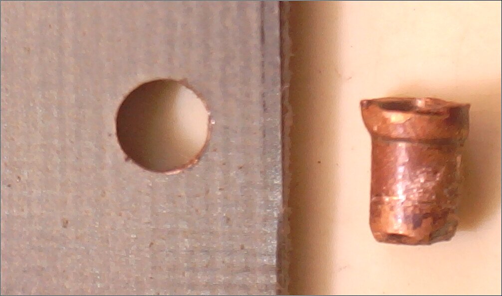
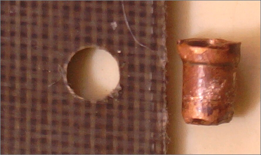
Rivets in 2.3mm hole in PCB
Rivet Flattened At Each End, Drilled (1.2mm) And Soldered
Liquid flux used, same as I use with SMT soldering. Then a quick rub with a fine wire brush to remove the gunk, hence the fine scratches. I’m testing the basic functionality at this point and not looking to win any beauty contests.
This is 1mm thick Teflon composite pcb material from a 5.6GHz antenna and the rivet is a bit too close to the edge which you can see has a small bulge from the rivet expanding as it was pressed. Next time I’ll anneal the rivet, fit it further from a edge and not squish it so much.
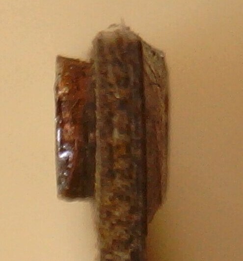
Rivet Edge View
Elm Chan
A beautiful example of precision hand wiring and soldering
This example taken from http://elm-chan.org/docs/wire/wiring_e.html
Note
If this method didn’t work, then the picture below (by Elm Chan) wouldn’t exist.
How to prepare thicker wire with much higher temperature enamel for soldering ?
Using a gas lighter (cigarette) or a match hold the small flame over the end of the wire which will blacken as the enamel burns off
Lightly sand the black off with fine sandpaper or use a knife, my favorite is my “three cornered scraper”
Solder coat the end with your iron as usual
PCB
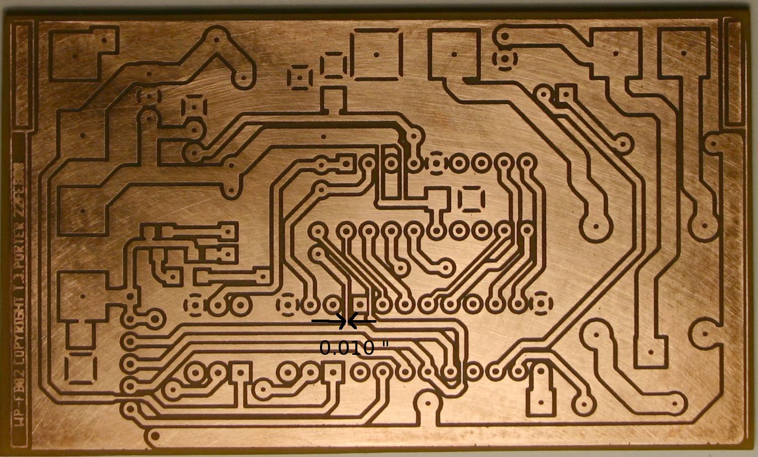
After a prototype has been completed and tested using the wiring method I then make up a PCB which I do in-house and looks something like the picture below.
This hand etched copper pcb sat in my leather wallet for about 10 years after I made it. I gave it a quick sanding as it was a bit green and corroded then took this picture.
Methods
I use simple techniques applied by hand for my single sided prototype pcbs.
Action |
Description |
|---|---|
Schematic Capture Software |
gEDA Gschem (GPL) http://www.geda-project.org |
PCB Cad Layout Software |
gEDA PCB (GPL) |
Copper |
With photo resist applied |
Artwork |
Laser printed on Drafting Film paper |
Exposure |
Light Box with Black Light fluro tubes |
Etchant |
Ferric Chloride heated and agitated |
Drilling |
Dremel high speed drill on a hand operated stand |
Drill Bits |
Carbide |
A deadbugged STM32F051, hand soldered
Running Mecrisp-Stellaris !