PCB Turret Pins
Brass, Solder Plated Turret Pins
Some have a castellated top that can be crimped before winding the lead/wire around the pin and soldering, adding even more strength to the assembly. Some have a serrated base designed to dig into the PCB so they cannot rotate. The price increases with pin complexity.
The main point is that brass/copper is strong, solder is very weak. Solder should never be relied upon to affix components by itself as it only provides electrical connectivity..

Typical Turret Pin Use
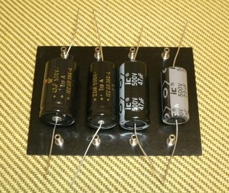
In this picture four electrolytic capacitors use the pins as mounting posts. The leads will be wrapped around the posts and then soldered. This provides a superior mounting for the capacitors with minimal bending of the leads coming from the caps. The alternate method used these days is to bend the leads and stick them thru the PCB, soldering to the copper tracks. This method is a source of problems as solder has no strength in itself and the caps are heavy, meaning that vibration from use or moving the equipment often creates hairline cracks in the solder joint resulting in electrical faults.
The turret pins also provide easy oscilloscope measuring points and external wire attachment. Once upon a time this method was very common in electronics equipment and will still be found in high end gear designed to last.
I’ve been making some turret pin punches so I can quickly prototype projects on mostly copperless 1mm thick Teflon composite PCB substrate recovered from faulty Chinese WiFi panel antennas.
I have a heap of these and the material is easy to work with and good for use at 5GHz.
My Turret Pins
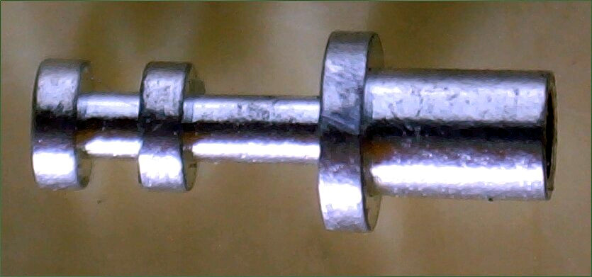
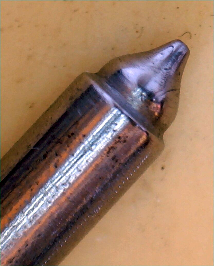
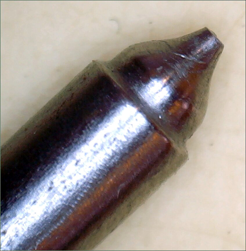
Firstly the turret pin I’m using. These are somewhat expensive at $0.205 AUD each for 200+. They have to be fitted in a 1.5mm hole in the PCB and then the base has to be expanded and flattened to strongly anchor the pin.
The long cylindrical bit on the right hand side is the base of the pin. The diameter is 1.55mm, and the hole inside is 0.8mm so yeah, it’s tiny. This is the part that has to be flared underneath the PCB.
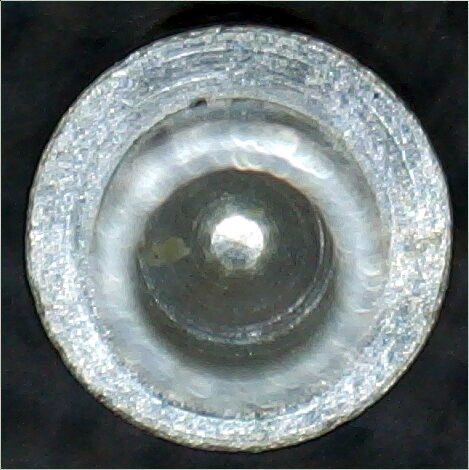
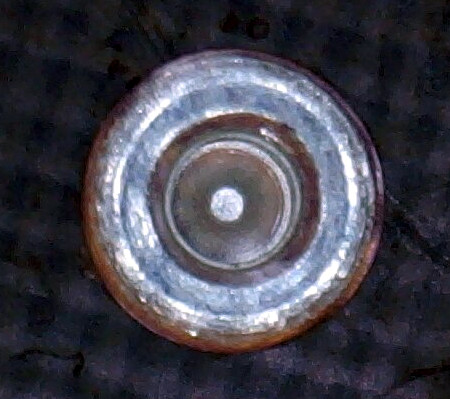
Pin Base End
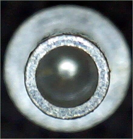
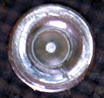
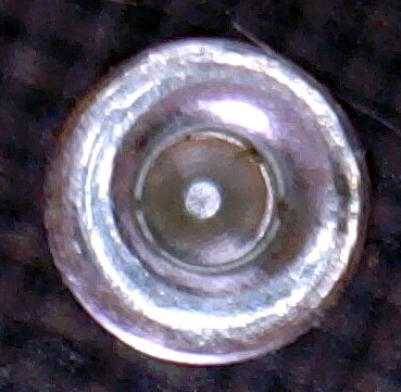
This picture shows a new pin, looking at the base.
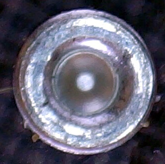
Pin Base Inner
The camera is focused at the bottom of the pin, inside the cylinder that is to be flared and flattened. The centre circular indent is part of the pin manufacturing process and not caused by my tools.
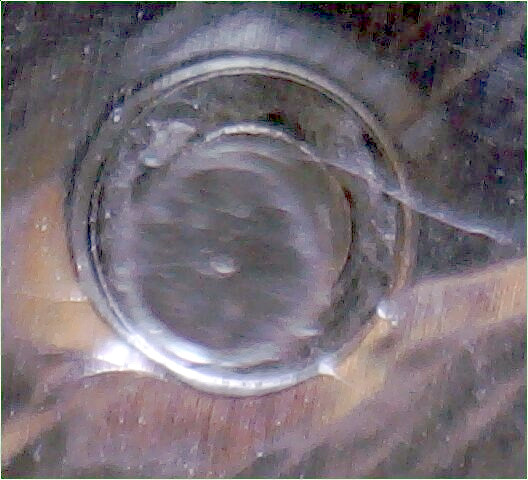
Flaring The Base
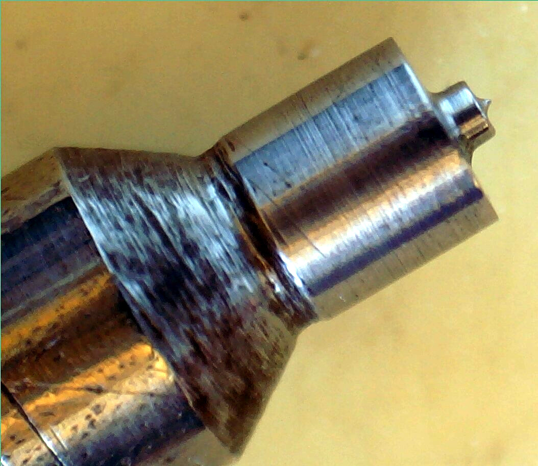
The all critical flaring of the pin base. No, not my first, second, third or later attempt, they’re too horrible to show here. This failed because it has two base splits, and I was still learning about the kind of tools I needed. This is the long cylindrical bit on the right hand side in the first picture, now flattened out.
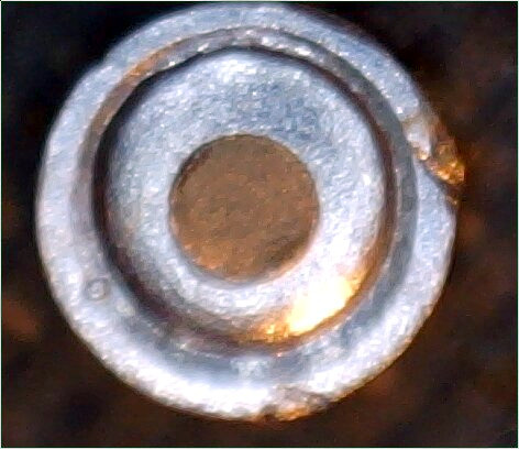
Success
Attempt number 22, flared and flattened. The tools were not smoothed and polished at this stage so it’s still very rough. The flare tool tip is too long and slightly cratering the base.
The tools
These are applied by hand and hammered down on the pin itself. I’m not using a pin press at the moment as I don’t think I need one due to my pin tool designs.
Tool #1, The Flare
I had to handmake this tool as the contours are curved. This was done on my small Chinese lathe by turning, filing, sanding, and polishing. The nose of this tool where it starts to curve up, is only 0.8mm in diameter and guides the tool into the pin base. Without it the tool could (and would) slide sideways and ruin the pin.
I use it to flare the pin base ready for tool #2 which is then used to flatten the base.
Initially the flare tool was penetrating about half a thousands of a inch too deep and cratering the inside of the pin (which can be seen above), so I removed about 1 thou from the tip of the tool which fixed the issue.
Sizing
It seems the tool dimensions aren’t critical as long as the nose of the tool fits inside the pin to guide it as it flares the base enough for tool #2 to flatten it, without splitting the flare first.
Flare Tool, too long
Flare Tool, shortened
This version made pins 1 - 4 below.
Tool #2, The Flattener
This tool was turned, then polished by hand with fine emery paper, Brasso polishing liquid etc, the same as Tool #1. The small cylindrical nose at the right hand side is 0.8mm in diameter and is used to register the tool with the hole in the base of the (now fared) pin and keep it aligned during the flattening process. I didn’t even see the tiny pointy bit on the end until I took this picture with my USB microscope, which I’ve left as a telltale to show if this tool is striking the inside base of the pin.
Sizing
This tool, apart from the small cylindrical nose used to guide the tool, has a completely flat face.
The Anvil
No picture as it’s just a piece of brass rod, with a hole of 1.55mm to accept the pin tower which is pushed into the anvil so only the pin base protrudes, ready to fit the pcb and then flare and flatten. The anvil is simply held in a standalone drill chuck on a base and sits on my workbench.
The Hammer
This is a small instrument type hammer and only a few firm taps are needed for each operation. I can feel when the flare tool has expanded the base and when the flattener has finished it’s job.
Final Crimps
Pins #3 and #4 have a more consistent squish which is just a matter of practice I think. The crimps are smoother, reflecting the (now) polished finish of the tool faces.
Than again, everything looks flawed in some way under a microscope!
Pin1
Pin2
Pin3
Pin4
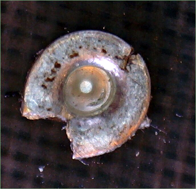
Results
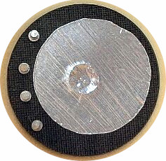
The pins are very securely affixed, don’t wiggle and can’t be removed by hand, in fact twisting the pin back and forth only resulted in the body of the pin breaking off, leaving the base still attached to the PCB as shown below. This is a picture from the top of the pin, showing the base.
Tested to Destruction
The copper circular area is whats left of the pin tower after it was twisted off with pliers which took several side to side twists.
This is a very secure component/wiring mounting method providing component legs/wires are twisted multiple times around the pin tower before being soldered.
Warning
This method naturally also makes the part/wire difficult to remove. I use a solder sucker tool to draw away all the solder and then unwind the joint from the pin tower, a method I learned dismantling WW2 surplus aircraft electronics gear as a kid.
Adhesive Backed Silver Paper
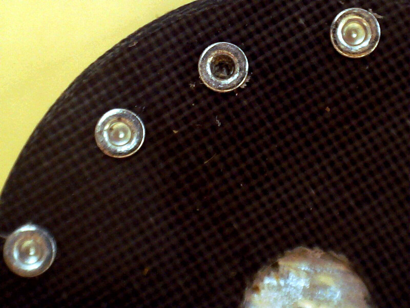
One may use adhesive backed silver paper on a PCB for various reasons, ground plane etc, so I’ve done the test. Here the silver paper is wrapped around both sides of the PCB and a turret pin fitted thru both layers.
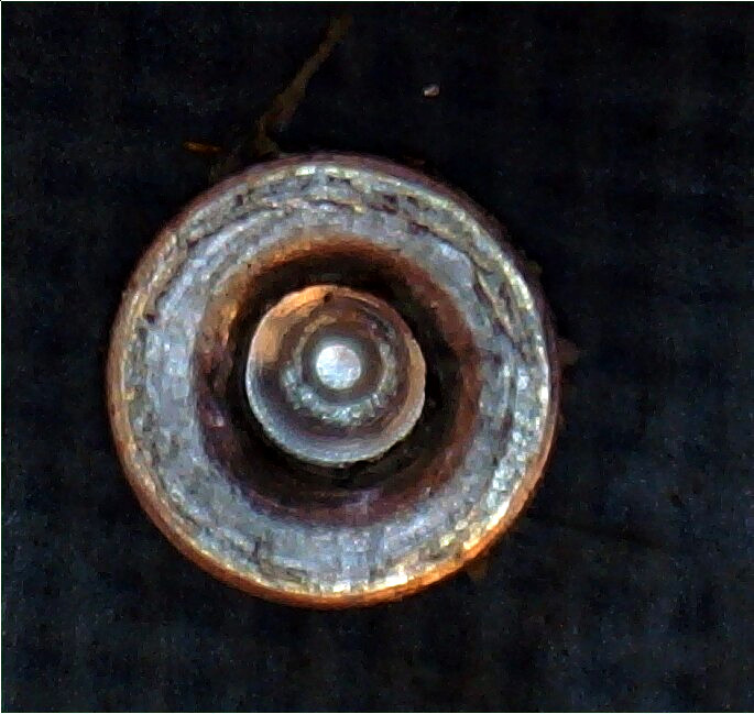
Turret
Although this USB microscope picture looks ok, the base of the pin has severed the aluminium foil all the way around the base. This is clearly seen under my 40 power binocular microscope.
Base
Very obvious here, the base has cut thru the foil.
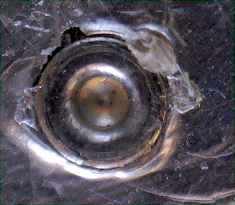
Conclusion
Total fail, unreliable electrical contact between pin and foil. The clamping force would need to be spread over a larger area with washers, however this would require a deeper pin base (on a different turret pin part) to allow for the extra washer thickness.
Alternate Pin Fitting
Found on YouTube 2021.
Drill Press
https://www.youtube.com/watch?v=iYtQC4UBysE
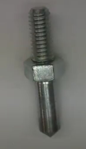
Bolt used as Flare Tool
This flare tool profile is easy to hand grind or turn on a lathe etc but it requires a drill press to use. One risks ruining the drill press bearings because the bearings used are not conical bearings and cannot stand much end-loading. Certainly pressing annealed copper turret pins is barely loading the drill press much anyway.
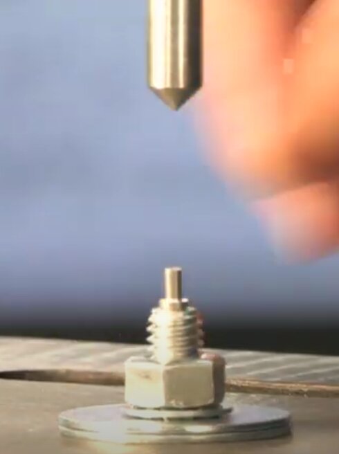
Combination
The full setup, flare and anvil with pin loaded.
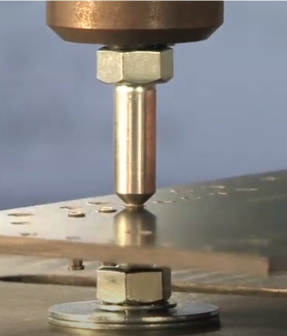
Final Product
Because only a flare tool is used, the base of the pin doesn’t look totally flat to me, and that means the pin isn’t as securely fixed as it could be if it were. A flattener tool could easily be made and used to hand hammer the base flat. A few taps with a small hammer are all that’s needed.
Building a Test PCB
The reason for making the pin turret tools is so I can quickly prototype electrically decent PCB’s at home in minimum time. No need to make a PCB CAD and send it to a fab then wait until it ships back. No waiting, no delay.
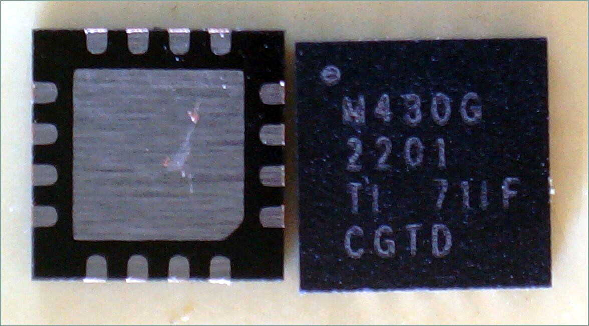
I want to test this chip with Mecrisp-Across and need to put it in a PCB to do that. The chip is 4 * 4 mm in size.
Firstly, I ran into a chip soldering problem see Out of Date QFN chips ? for details.
Now onto the PCB!
Why Not Use a Plug In BreadBoard ?
DIP use only, NO header pins !
Pcb headers jammed into breadboard makes later IC connections and gripping in same locations very weak. - BAD
Connections provide the mounting - BAD
Vibration can cause connections faults - BAD
High capacitance
High inductance
no ground plane, lots of noise and mains hum
Only cheap junk available now. A high quality plug in board with gold plated wipers is very expensive … if you can find one.
Low current capacity
Forget about developing low noise or high speed circuits on one.
Forget about reliability
Having said all that, this one by National Instruments is probably well designed, the price is $5500.00 AUD.
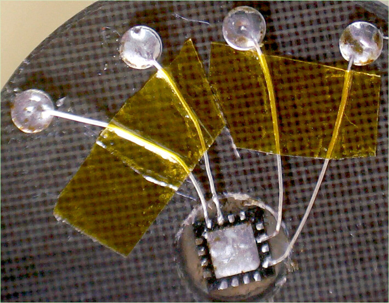
PCB Top
The pcb was roughly cut out, the 6.5mm centre hole for the chip was drilled then rounded on the lathe using a mandrel in the centre hole. The silver disc (hand cut with scissors from a roll of adhesive backed silver tape from Aldi stores) was attached. Four holes were drilled in the drill press and turret pins were then easily fitted. Four light hammer taps on each of the two tools (for each pin) and I had perfect crimps as you can see.
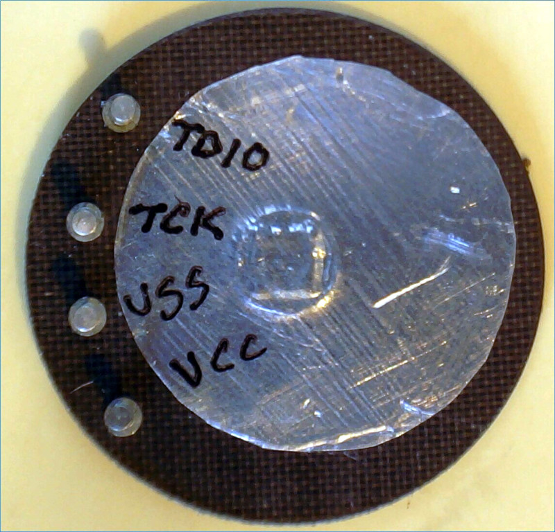
PCB Bottom
Note to self, temporally tape over open hole before fitting pins to keep out debris.
PCB With MCU
A SMALL board.
The KEY to doing a job like this is having the right parts and equipment.
Parts/Equipment
Hand tinned 16 pin QFN chip by Ti
Binocular microscope of 40x used for soldering as my eyes are 67 years old.
Recycled Teflon composite PCB material from faulty 5.8GHz WiFI pannel antennas. Fibreglass and phenolic can be used instead.
Kapton tape is used to hold wire in position for soldering
Aluminium adhesive tape is used to affix the chip inside the PCB hole as it’s a great heatsink during soldering. It’s also quite strong and cheap. Initially I used Kapton tape but the chip became so hot while soldering that the adhesive lost all strength and the chip came loose along with the Kapton.
Wire: is rather unique being at least fifty (50) years old ! I stripped all the parts from an old Burroughs B5000 tape drive around 1985 including a lot of blue coloured Teflon insulated multi strand wire. One strand of that wire is used here and is 0.020 mm in diameter or 52 AWG. It’s very soft, I think it’s silver plated copper and is the easiest wire to solder I’ve ever used. No liquid flux is needed.
Thermaltronics TMT-900S-2 soldering iron with a 1mm conical tip. Very old one mm resin cored solder (containing lead) used.
Bottom
Finished Top
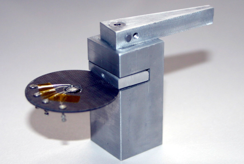
Home Made PCB Vice
It’s designed for soldering and working on small pcbs under a Binocular Microscope
Turning the arm one quarter turn clockwise lowers the ‘foot’ onto the pcb and locks it so it can’t move. Made on a lathe and milling machine.
Ready To Test
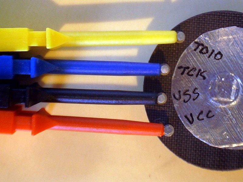
Working
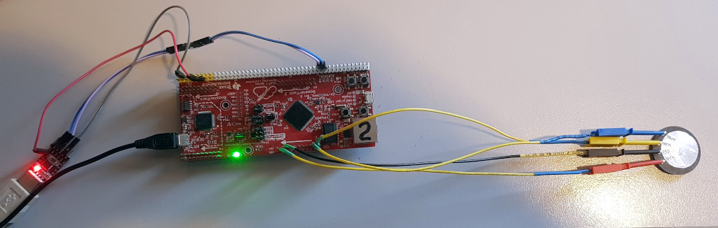
25.10.2021: Yes it works, first time, even without a local cap across VCC and VSS :)
Mecrisp-Stellaris 2.4.5 (tpMOD:cr,rts,480600) for TM4C1294 by Matthias Koch
emu Connecting to target in emulation mode
Board Response
The chip is a MSP430G2201 but we only get the last three digits from Mecrisp-Across.
Chip erkannt: F201
Ruggedness ?
When the PCB is tested and working, a layer of adhesive protection such as clothtape will cover the entire underneath of the PCB.
The MCU is stuck to the aluminum adhesive so it won’t move. If it was going into a harsh environment and needed additional ruggedness, I would fill in the hole (and chip) with a non hardening adhesive filler such as “Bear Cement”.
Once it cures, while not hard, it is incredibly tenacious.